LTC3226
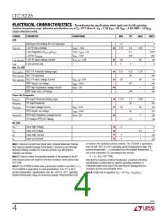
ELECTRICAL CHARACTERISTICS The l denotes the specifications which apply over the full operating
junction temperature range, otherwise specifications are at TA = 25°C (Note 3). VIN = 3.3V, VCPO = 5V, VOUT = 3.3V, VMID = 1/2 VCPO
unless otherwise noted.
SYMBOL
LDO
PARAMETER
CONDITIONS
MIN
TYP
MAX
0.82
60
UNITS
Minimum CPO Voltage for LDO Operation
LDO FB Servo Voltage
2.4
V
V
l
l
V
I
= 1mA
0.76
0.8
2.7
200
LDO_FB
VOUT
Load Regulation ΔV
/ΔI
1mA < I
< 2A
VOUT
mV/A
mΩ
nA
LDO_FB OUT
LDO FET R
V
= 3.6V
CPO
DS(ON)
I
I
LDO_FB Input Leakage Current
LDO Current Limit
V
= 0.9V
–60
2
LDO_FB(LEAK)
LDO_FB
4
A
LIM
RST_FB, RST
l
l
l
V
V
RST_FB Threshold (Falling Edge)
RST_FB Hysteresis
0.72
–50
0.74
20
0.76
50
1
V
mV
nA
RST_FB(TH)
RST_FB(HYS)
RST_FB(LEAK)
I
RST_FB Input Leakage Current
RST Output Low Voltage
V
= 0.9V
RST_FB
I
= 5mA
65
mV
ꢀA
SINK
RST High Impedance Leakage Current
RST Delay (RST_FB Rising)
V = 5V
RST
290
ms
Power-Fail Comparator
l
l
l
V
V
PFI Input Threshold (Falling Edge)
PFI input Hysteresis
1.175
–50
1.2
20
1.225
50
V
mV
nA
PFI(TH)
PFI(HYS)
PFI(LEAK)
I
PFI Input Leakage Current
V
= 0.5V
PFI
PFO Output Low Voltage
I
= 5mA
= 5V
65
mV
ꢀA
SINK
I
)
PFO High Impedance Leakage Current
PFI Delay to PFO (PFI Falling)
V
PFO
1
PFO(LEAK
0.5
ꢀs
EN_CHG
l
l
l
l
V
V
Input High Voltage
Input Low Voltage
Input High Current
Input Low Current
1.3
V
V
IH
IL
0.4
1
I
IH
I
IL
–1
–1
ꢀA
ꢀA
1
correlation with statistical process controls. The LTC3226I is guaranteed
over the full –40°C to 125°C operating junction temperature range. The
junction temperature, T , is calculated from the ambient temperature, T ,
Note 1: Stresses beyond those listed under Absolute Maximum Ratings
may cause permanent damage to the device. Exposure to any Absolute
Maximum Rating condition for extended periods may affect device
reliability and lifetime.
J
A
and power dissipation, P , according to the formula:
D
T = T + (P • 58.7°C/W)
Note 2: Failure to solder the exposed backside of the package to the PC
board ground plane will result in a thermal resistance much greater than
58.7°C/W.
J
A
D
Note that the maximum ambient temperature consistent with these
specifications is determined by specific operating conditions in
conjunction with board layout, the rated thermal package thermal
resistance and the environmental factor.
Note 3: The LTC3226 is tested under pulsed load conditions such that T ≈ T .
A
J
The LTC3226E is guaranteed to meet specifications from 0°C to 85°C
junction temperature. Specifications over the –40°C to 125°C operating
junction temperature range are assured by design, characterization and
Note 4: Output not in regulation; R = (2 • V – V )/I .
CPO CPO
OL
IN
3226fa
4

 Linear Systems [ Linear Systems ]