LTC3226
APPLICATIONS INFORMATION
where V is the forward voltage of the diode. As an ex-
GND is needed to set V
and the reset threshold 7.5%
F
OUT
ample, if R
= 200k, R
= 120k, R = 2M, and V =
PF2 H F
below the V
programmed voltage. However, the reset
PF1
OUT
0.4V, the additional hysteresis provided by this network
can be calculated using the above equation as follows:
threshold can be set independent of V
resistor divider.
by an additional
OUT
200kΩ
2MΩ
Effective Open-Loop Output Resistance (R ) of the
ΔV
= 1.2+0.02–0.4 V •
= 82mV
OL
(
)
IN(HYS)
Charge Pump
Theeffectiveopen-loopoutputresistance(R )ofacharge
OL
V
V
OUT
IN
pumpdeterminesthestrengthofachargepump.Thevalue
470k
R
R
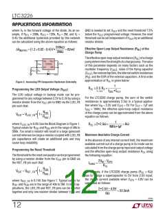
LTC3226
PFI
PF1
H
of this parameter depends on many factors such as the
PFO
oscillator frequency (f ), value of the flying capacitor
OSC
R
PF2
D1
(C ),thenonoverlaptime,theinternalswitchresistances
FLY
3226 F02
(R ), and the ESR of the external capacitors. A first order
S
approximation of R is given below:
OL
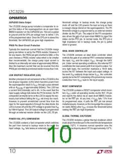
Figure 2. Increasing PFI Comparator Hysteresis Externally
1
ROL ≅ 2 Σ RS +
Programming the LDO Output Voltage (V
)
OUT
fOSC •CFLY
S=1to4
The LDO output voltage in backup mode can be pro-
grammed for any voltage between 2.5V to 5.3V by using a
For the LTC3226 charge pump, the sum of the switch
resistances is approximately 2.5Ω in a typical applica-
resistor divider from the V
pin such that:
pin to GND via the LDO_FB
OUT
tion where V = 3.3V and V
= 5V. For C = 1ꢀF and
IN
CPO
FLY
f
= 1MHz, the effective open-loop output resistance
of the charge pump can be approximated from the above
OSC
⎛
⎜
⎝
⎞
RFB1
RFB2
VOUT = VLDO_FB • 1+
⎟
equation as follows:
⎠
1
where V
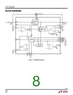
is 0.8V. See the Block Diagram in Figure 1.
ROL ≅ 2•2.5Ω+
= 6Ω
LDO_FB
1MHz • 1µF
Typical values for R and R are in the range of 40k to
FB1
FB2
500k. Too small a resistor will result in a large quiescent
current whereas too large a resistor coupled with LDO_FB
pin capacitance will create an additional pole and may
cause loop instability.
Maximum Available Charge Current
In the absence of any internal current limit, the maximum
available current out of a charge pump in 2x mode can be
calculated from the charge pump input and output voltage
and the effective open-loop output resistance R using
the following equation:
Programming the Reset Threshold
OL
Thethresholdfortheresetcomparatorcanbeprogrammed
by using a resistor divider from the V
the RST_FB pin such that:
pin to GND via
OUT
2V – VCPO
IN
ICHRG
=
ROL
⎛
⎜
⎝
⎞
RFB1
RFB2
VOUT = VRST _FB • 1+
For example, if the LTC3226 charge pump (R ≅ 6Ω)
has to charge a supercapacitor to 5V from 2.5V input,
the charge current available when V
calculated as follows:
⎟
OL
⎠
= 4.8V can be
CPO
where V
FB1
is 0.74V. See Figure 1. Typical values for
RST_FB
R
and R are in the range of 40k to 5M. In most ap-
FB3
plications, the LDO_FB and RST_FB pins can be shorted
together and only one resistor divider between V
2•2.5V – 4.8V
ICHRG
=
= 33.3mA
and
OUT
6Ω
3226fa
12

 Linear Systems [ Linear Systems ]