LTC3703
applicaTions inForMaTion
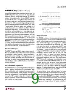
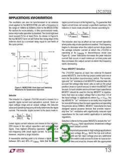
The oscillator can also be synchronized to an external
clock applied to the MODE/SYNC pin with a frequency in
the range of 100kHz to 600kHz (refer to the MODE/SYNC
Pin section for more details). In this synchronized mode,
pulse-skipmodeoperationisdisabled.Theclockhighlevel
must exceed 2V for at least 25ns. As shown in Figure 8,
the top MOSFET turn-on will follow the rising edge of the
external clock by a constant delay equal to one-tenth of
the cycle period.
ripple current occurs at the highest V . To guarantee that
IN
ripple current does not exceed a specified maximum, the
inductor in buck mode should be chosen according to:
V
V
OUT
V
IN(MAX)
OUT
L ≥
1–
f ∆I
L(MAX)
The inductor also has an affect on low current operation
whenpulse-skipmodeoperationisenabled.Thefrequency
begins to decrease when the output current drops below
the average inductor current at which the LTC3703 is
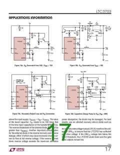
2V TO 10V
operating at its t
in discontinuous mode (see
MODE/
SYNC
ON(MIN)
Figure 6). Lower inductance increases the peak inductor
current that occurs in each minimum on-time pulse and
thus increases the output current at which the frequency
starts decreasing.
t
= 25ns
MIN
0.8T
T
T = 1/f
O
TG
D = 40%
0.1T
Power MOSFET Selection
The LTC3703 requires at least two external N-channel
power MOSFETs, one for the top (main) switch and one or
more for the bottom (synchronous) switch. The number,
type and “on” resistance of all MOSFETs selected take into
account the voltage step-down ratio as well as the actual
position (main or synchronous) in which the MOSFET will
beused.Amuchsmallerandmuchlowerinputcapacitance
MOSFET should be used for the top MOSFET in applica-
tions that have an output voltage that is less than 1/3 of
I
L
3703 F08
Figure 8. MODE/SYNC Clock Input and Switching
Waveforms for Synchronous Operation
Inductor
the input voltage. In applications where V >> V , the
IN
OUT
The inductor in a typical LTC3703 circuit is chosen for a
specific ripple current and saturation current. Given an
input voltage range and an output voltage, the inductor
valueandoperatingfrequencydirectlydeterminetheripple
current. The inductor ripple current in the buck mode is:
top MOSFETs’ “on” resistance is normally less important
foroverallefficiencythanitsinputcapacitanceatoperating
frequencies above 300kHz. MOSFET manufacturers have
designed special purpose devices that provide reason-
ably low “on” resistance with significantly reduced input
capacitance for the main switch application in switching
regulators.
VOUT
(f)(L)
VOUT
∆IL =
1–
V
IN
Selection criteria for the power MOSFETs include the “on”
Lower ripple current reduces core losses in the inductor,
ESR losses in the output capacitors and output voltage
ripple. Thus highest efficiency operation is obtained at
low frequency with small ripple current. To achieve this
however, requires a large inductor.
resistance R
, input capacitance, breakdown voltage
DS(ON)
and maximum output current.
Themostimportantparameterinhighvoltageapplications
is breakdown voltage BV . Both the top and bottom
DSS
MOSFETs will see full input voltage plus any additional
ringing on the switch node across its drain-to-source dur-
ing its off-time and must be chosen with the appropriate
A reasonable starting point is to choose a ripple current
between 20% and 40% of I
. Note that the largest
O(MAX)
3703fc
13

 Linear Systems [ Linear Systems ]