Specifications GAL20V8Z
Specifications GAL20V8Z
GAL20V8ZD
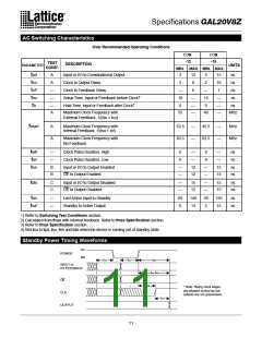
AC Switching Characteristics
Over Recommended Operating Conditions
COM
-12
COM
-15
TEST
DESCRIPTION
PARAMETER
UNITS
COND1.
MIN. MAX.
MIN. MAX.
tpd
tco
tcf2
tsu
th
A
A
Input or I/O to Combinational Output
3
2
12
8
3
2
15
10
7
ns
ns
ns
ns
Clock to Output Delay
—
—
Clock to Feedback Delay
—
10
6
—
15
Setup Time, Input or Feedback before Clock↑
Hold Time, Input or Feedback after Clock↑
—
—
—
A
0
—
—
0
—
—
ns
Maximum Clock Frequency with
External Feedback, 1/(tsu + tco)
55
40
MHz
fmax3
A
A
Maximum Clock Frequency with
Internal Feedback, 1/(tsu + tcf)
62.5
83.3
—
—
45.5
62.5
—
—
MHz
MHz
Maximum Clock Frequency with
No Feedback
twh
twl
—
—
Clock Pulse Duration, High
Clock Pulse Duration, Low
6
6
—
—
8
8
—
—
ns
ns
ten
B
B
Input or I/O to Output Enabled
OE to Output Enabled
—
—
12
12
—
—
15
15
ns
ns
tdis
C
C
Input or I/O to Output Disabled
OE to Output Disabled
—
—
15
12
—
—
15
15
ns
ns
tas
tsa4
—
—
Last Active Input to Standby
Standby to Active Output
60
6
140
13
50
5
150
15
ns
ns
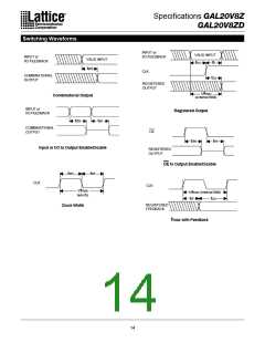
1) Refer to Switching Test Conditions section.
2) Calculated from fmax with internal feedback. Refer to fmax Specification section.
3) Refer to fmax Specification section.
4) Add tsa to tpd, tsu, ten and tdis when the device is coming out of standby state.
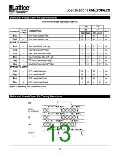
Standby Power Timing Waveforms
Icc
POWER
Isb
t
as
t
sa
tpd
INPUT or
I/O FEEDBACK
t
en, tdis
OE
t
su
*
* Note: Rising clock edges
are allowed during sa but
outputs are not guaranteed.
t
CLK
t
co
OUTPUT
11

 LATTICE [ LATTICE SEMICONDUCTOR ]