Pinout Information
LatticeECP2/M Family Data Sheet
Lattice Semiconductor
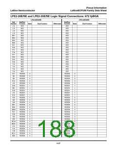
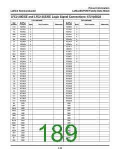
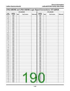
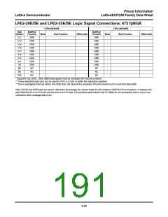
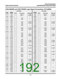
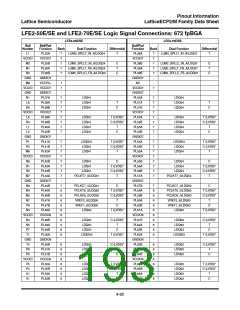
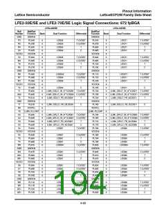
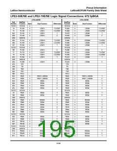
LFE2-20E/SE and LFE2-35E/SE Logic Signal Connections: 672 fpBGA
LFE2-20E/20SE
LFE2-35E/35SE
Ball
Number
Ball/Pad
Function
Ball/Pad
Function
Bank Dual Function
Differential
Bank
Dual Function
Differential
U11
U13
U14
U16
U17
V13
V14
V21
V6
GND
GND
GND
GND
GND
GND
GND
GND
GND
NC
-
-
-
-
-
-
-
-
-
-
-
-
GND
GND
GND
GND
GND
GND
GND
GND
GND
NC
-
-
-
-
-
-
-
-
-
-
-
-
M3
N6
NC
NC
P24
NC
NC
* Supports true LVDS. Other differential signals must be emulated with external resistors.
** These dedicated input pins can be used for GPLLs or GDLLs within the respective quadrant.
***Due to packaging bond out option, this DQS does not have all the necessary DQ pins bonded out for a full 8-bit data width.
Note:VCCIO and GND pads are used to determine the average DC current drawn by I/Os between GND/VCCIO connections, or between the
last GND/VCCIO in an I/O bank and the end of an I/O bank. The substrate pads listed in the Pin Table do not necessarily have a one to one
connection with a package ball or pin.
4-90

 LATTICE [ LATTICE SEMICONDUCTOR ]