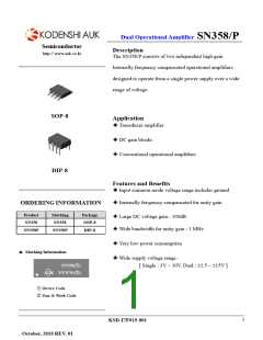
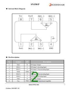
SN358/P
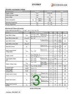
Absolute maximum ratings
Characteristic
Symbol
VCC
Ratings
36 or ±18
32
Unit
V
Supply voltage
Differential input voltage
Input voltage
VIND
V
VIN
-0.3 ~ +32
600
V
SOP-8
mW
mW
°C
Power Dissipation
PD
DIP-8
1000
Operating temperature
Storage temperature
-45 ~ +85
-55 ~ 150
Topr
Tstg
°C
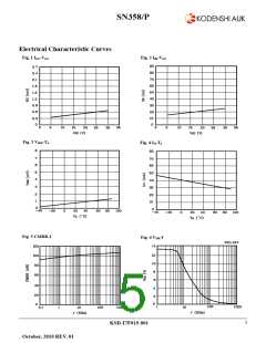
Electrical Characteristics
(Unless otherwise specified. VCC = 5V and –45 °C ≤ Ta ≤ +85 °C)
Characteristic
Symbol
Test Condition
Min. Typ. Max.
Unit
-
-
-
-
-
-
-
-
5V ≤ VCC ≤ 30V
(Ta=25 °C)
±2
-
±7
Input offset voltage
VIOS
mV
Rg = 0Ω, 0V ≤ VIC ≤ VCC-1.5V
Rg = 0Ω
±9
-
Input offset voltage drift
Input offset current
7
ΔVIOS/ΔT
μV/ °C
(Ta=25 °C)
±5
±50
±150
-
IIOS
-
nA
Input offset current drift
Input bias current
-
10
45
40
ΔIIOS/ΔT
pA/ °C
250
500
(Ta=25 °C)
IIB
-
nA
VCC
–1.5
VCC
–2
0
0
-
-
V
V
(Ta=25 °C)
Input common mode
voltage range
VICR
VCC = 30V
-
1
0.7
100
-
2
1.2
-
VCC = 30V, RL = ∞
Supply current
ICC
GV
mA
V/mV
V
-
V
CC = 5V, RL = ∞
25
15
26
27
-
(Ta=25 °C)
V
CC = 15V
Large signal voltage
gain
RL ≥ 2 KΩ
-
VCC = 30V
-
-
RL=2 KΩ
VOH
Output voltage swing
28
3
-
RL=10 KΩ
VOL
20
mV
dB
V
CC =5V, RL ≤10 KΩ
Common mode
rejection ratio
Power supply
rejection ratio
CMRR
65
65
90
-
-
(Ta=25 °C)
PSRR
IO+
100
dB
(Ta=25 °C)
VCC = 15V
20
10
10
5
40
20
20
8
-
-
-
-
(Ta=25 °C)
(Ta=25 °C)
(Ta=25 °C)
Output source current
mA
V
IN+ = 1V, VIN- = 0V
VCC = 15V
mA
VIN+ = 0V, VIN- = 1V
VOUT = 200mV,
VIN+ = 0V, VIN- = 1V
Output sink current
IO-
12
-
50
40
-
μA
Output short circuit to
ground
ISC
60
mA
Ta=25 °C
3
KSD-I7F015-001
October, 2010 REV. 01

 KODENSHI [ KODENSHI KOREA CORP. ]