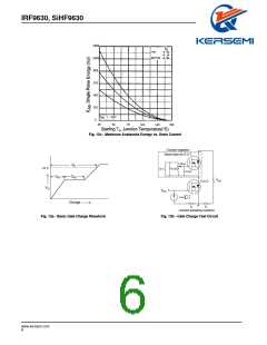
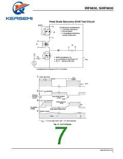
IRF9630, SiHF9630
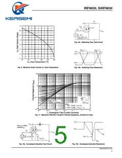
RD
VDS
VGS
D.U.T.
RG
+
-
V
DD
- 10 V
Pulse width ≤ 1 µs
Duty factor ≤ 0.1 %
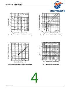
Fig. 10a - Switching Time Test Circuit
td(on) tr
td(off) tf
VGS
10 %
90 %
VDS
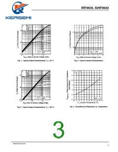
Fig. 9 - Maximum Drain Current vs. Case Temperature
Fig. 10b - Switching Time Waveforms
Fig. 11 - Maximum Effective Transient Thermal Impedance, Junction-to-Case
IAS
L
VDS
Vary tp to obtain
required IAS
VDS
D.U.T
IAS
RG
-
V
+
DD
VDD
tp
- 10 V
A
0.01 Ω
tp
VDS
Fig. 12b - Unclamped Inductive Waveforms
Fig. 12a - Unclamped Inductive Test Circuit
www.kersemi.com
5

 KERSEMI [ Kersemi Electronic Co., Ltd. ]