IXTU 01N80
IXTY 01N80
Symbol
gfs
TestConditions
Characteristic Values
(TJ = 25°C, unless otherwise specified)
min. typ. max.
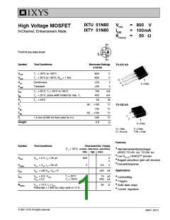
TO-251 AA Outline
VDS = 10 V; ID = 0.5 ID25, pulse test
140
mS
Ciss
Coss
Crss
60
8.0
2.0
pF
pF
pF
VGS = 0 V, VDS = 25 V, f = 1 MHz
td(on)
tr
td(off)
tf
12
12
28
28
ns
ns
ns
ns
1. Gate
2. Drain
3. Source
4. Drain
VGS = 10 V, VDS = 500 V, ID = ID25
Back heatsink
RG = 50 Ω (External)
Dim.
Millimeter
Inches
Min.
Max.
Min.
Max.
A
2.19
0.89
2.38
1.14
.086
0.35
.094
.045
Qg(on)
Qgs
8
1.8
3
nC
nC
nC
A1
b
0.64
0.76
5.21
0.89
1.14
5.46
.025
.030
.205
.035
.045
.215
VGS = 10 V, VDS = 0.5 VDSS, ID = 0.5 ID25
b1
b2
Qgd
c
0.46
0.46
0.58
0.58
.018
.018
.023
.023
c1
RthJC
3
K/W
D
5.97
6.22
.235
.245
E
6.35
2.28
4.57
6.73
BSC
BSC
.250
.090
.180
.265
BSC
BSC
e
e1
H
17.02
17.78
.670
.700
L
8.89
1.91
0.89
1.15
9.65
2.28
1.27
1.52
.350
.075
.035
.045
.380
.090
.050
.060
L1
L2
L3
Source-DrainDiode
Characteristic Values
(TJ = 25°C, unless otherwise specified)
min. typ. max.
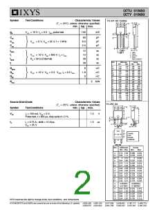
TO-252 AA
Symbol
VSD
TestConditions
IF = 100 mA, VGS = 0 V,
Pulse test, t ≤ 300 µs, duty cycle d ≤ 2 %
1.5
V
trr
IF = 0.75 A, -di/dt = 10 A/µs,
VDS = 25 V
1.5 µs
1Anode
2 NC
3Anode
4 Cathode
Dim.
A
Millimeter
Min. Max. Min.
Inches
Max.
2.19 2.38 0.086 0.094
A1 0.89 1.14 0.035 0.045
A2
b
0
0.13
0
0.64 0.89 0.025 0.035
0.005
b1
b2
0.76 1.14 0.030 0.045
5.21 5.46 0.205 0.215
c
c1
0.46 0.58 0.018 0.023
0.46 0.58 0.018 0.023
D
D1
5.97 6.22 0.235 0.245
4.32 5.21 0.170 0.205
E
E1
6.35 6.73 0.250 0.265
4.32 5.21 0.170 0.205
e
e1
2.28 BSC
4.57 BSC
0.090BSC
0.180BSC
H
L
9.40 10.42 0.370 0.410
0.51 1.02 0.020 0.040
L1
L2
L3
0.64 1.02 0.025 0.040
0.89 1.27 0.035 0.050
2.54 2.92 0.100 0.115
IXYS reserves the right to change limits, test conditions, and dimensions.
IXYS MOSFETS and IGBTs are covered by one or more of the following U.S. patents: 4,835,592 4,881,106
4,850,072 4,931,844
5,017,508
5,034,796
5,049,961 5,187,117 5,486,715
5,063,307 5,237,481 5,381,025

 IXYS [ IXYS CORPORATION ]