欢迎访问ic37.com |
会员登录 免费注册
发布采购

IT7001M 参数 Datasheet PDF下载

IT7001M图片预览
型号: IT7001M
PDF下载: 下载PDF文件 查看货源
内容描述: 可编程的8位二进制计数器,同步预设启用 [Programmable 8-Bit Binary Counter with Synchronous Preset Enable]
分类和应用: 计数器
文件页数/大小: 24 页 / 218 K
品牌: ITE [ ITE TECH.INC. ]
 浏览型号IT7001M的Datasheet PDF文件第1页浏览型号IT7001M的Datasheet PDF文件第3页浏览型号IT7001M的Datasheet PDF文件第4页浏览型号IT7001M的Datasheet PDF文件第5页浏览型号IT7001M的Datasheet PDF文件第6页浏览型号IT7001M的Datasheet PDF文件第7页浏览型号IT7001M的Datasheet PDF文件第8页浏览型号IT7001M的Datasheet PDF文件第9页  
Copyright ã 2000 ITE, Inc.  
This is Preliminary document release. All specifications are subject to change without notice.  
The material contained in this document supersedes all previous documentation issued for the related products  
included herein. Please contact ITE, Inc. for the latest document(s).  
All sales are subject to ITE’ s Standard Terms and Conditions, a copy of which is included in the back of this  
document.  
ITE, IT7001M/IT7001N is a trademark of ITE, Inc.  
All other trademarks are claimed by their respective owners.  
All specifications are subject to change without notice.  
Additional copies of this manual or other ITE literature may be obtained from:  
ITE (USA) Inc.  
Phone: (408) 530-8860  
Fax: (408) 530-8861  
Marketing Department  
1235 Midas Way  
Sunnyvale, CA 94086  
U.S.A.  
ITE (USA) Inc.  
Phone: (512) 388-7880  
Fax: (512) 388-3108  
Eastern U.S.A. Sales Office  
896 Summit St., #105  
Round Rock, TX 78664  
U.S.A.  
ITE, Inc.  
Marketing Department  
Phone: (02) 2657-9896  
Fax: (02) 2657-8561, 2657-8576  
7F, No. 435, Nei Hu District, Jui Kuang Rd.,  
Taipei 114, Taiwan, R.O.C.  
If you have any marketing or sales questions, please contact:  
Lawrence Liu, at ITE Taiwan: E-mail: lawrence.liu@ite.com.tw, Tel: 886-2-26579896 X6071,  
Fax: 886-2-26578561  
David Lin, at ITE U.S.A: E-mail: david.lin@iteusa.com, Tel: (408) 530-8860 X238,  
Fax: (408) 530-8861  
Don Gardenhire, at ITE Eastern USA Office: E-mail: don.gardenhire@iteusa.com  
Tel: (512) 388-7880, Fax: (512) 388-3108  
To find out more about ITE, visit our World Wide Web at:  
http://www.ite.com.tw  
http://www.iteusa.com  
Or email itesupport@ite.com.tw for more product information/services.  
Revision History  
Revision History  
Section  
Revision  
Page No.  
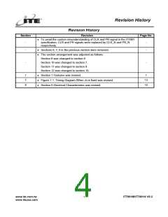
l To avoid the custom misunderstanding of CLR and PR signal in the IT7001  
specification, CLR and PR signals were replaced by CLR_N and PR_N  
respectively.  
-
-
-
-
l Sections 6, 7, 8 in the previous version were removed.  
l The section arrangement was adjusted as follows:  
Section 9 was changed to section 6.  
-
Section 10 was changed to section 7.  
Section 11 was changed to section 9.  
Section 12 was changed to section 10.  
-
1
7
8
l Section 1 Features was revised.  
1
13  
15  
l Figure 7-1. Timing Diagram When Jn is fixed was revised.  
l Section 8 Electrical Characteristics was revised.  
www.ite.com.tw  
www.iteusa.com  
IT7001M/IT7001N V0.2  
1
Contents  
CONTENTS  
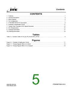
1. Features...................................................................................................................................................1  
2. General Description..................................................................................................................................3  
3. Block Diagram..........................................................................................................................................5  
4. Pin Configuration......................................................................................................................................7  
5. IT7001M/IT7001N Pin Description ............................................................................................................9  
6. Example of Application Circuit ................................................................................................................11  
7. Timing Chart: Example of AC Signal Generator ......................................................................................13  
8. DC Characteristics..................................................................................................................................15  
9. Package Information...............................................................................................................................17  
10.Ordering Information...............................................................................................................................19  
Tables  
Table 5-1. Function Table of CLR_N, PR_N and SPE_N Pins........................................................................9  
Figures  
Figure 6-1. Example of Application Circuit....................................................................................................11  
Figure 7-1. Timing Diagram When Jn is fixed...............................................................................................13  
Figure 7-2. Timing Diagram When Jn is changed .........................................................................................14  
www.ite.com.tw  
www.iteusa.com  
IT7001M/IT7001N V0.2  
i
Features  
1. Features  
n Wide Operation Voltage  
-
Vcc = 2.5 to 5.5 V  
n Low Static Current (Ta = 25  
Icc (Static) = 10 mA (max)  
n Package:  
°C)  
-
-
IT7001M: 16-SOP  
-
IT7001N: 16-TSSOP  
www.ite.com.tw  
www.iteusa.com  
Specifications Subject to Change without Notice  
IT7001M/IT7001N V0.2  
By Felix Sun, 12/18/2000  
ITPM-PN-200045  
1
www.ite.com.tw  
www.iteusa.com  
IT7001M/IT7001N V0.2  
2
General Description  
2. General Description  
The IT7001M/IT7001N consists of 8-bit binary down counter and D-type Flip Flop. The counter can set up to  
max 256 counts and synchronous preset (SPE_N) input can preset the data. When the count value is 0, the  
next clock pulse presets the data to invert the output. D-type Flip Flop takes the counter output as clock pulse,  
whose data is transferred to output at the rising edge. It is applied to generate AC signal for STN-type liquid  
crystal and divider for general usage.  
www.ite.com.tw  
www.iteusa.com  
IT7001M/IT7001N V0.2  
3
www.ite.com.tw  
www.iteusa.com  
IT7001M/IT7001N V0.2  
4
Logic Diagram  
3. Block Diagram  
CLK_N  
CLK  
J0  
J1  
J2  
J3  
J4  
J5  
J6  
J7  
J0  
J1  
J2  
J3  
J4  
J5  
J6  
J7  
CLK  
PR_N  
PR  
Q_N  
Q
D
CO_N  
CK  
Q
CLR  
SPE_N  
SPE_N  
CLR_N  
www.ite.com.tw  
www.iteusa.com  
IT7001M/IT7001N V0.2  
5
www.ite.com.tw  
www.iteusa.com  
IT7001M/IT7001N V0.2  
6
Pin Configuration  
4. Pin Configuration  
J0  
J1  
J2  
J3  
J4  
J5  
J6  
Vcc  
1
2
3
4
5
6
7
8
16  
15  
14  
13  
12  
11  
10  
9
CLK_N  
CLK  
Q
IT7001M/N  
PR_N  
SPE_N  
CLR_N  
J7  
GND  
Top View  
www.ite.com.tw  
www.iteusa.com  
IT7001M/IT7001N V0.2  
7
www.ite.com.tw  
www.iteusa.com  
IT7001M/IT7001N V0.2  
8
IT7001M/IT7001N Pin Description  
5. IT7001M/IT7001N Pin Description  
Signal  
VCC  
Pin(s) No.  
16  
Attribute  
Description  
Power  
¾
¾
I
GND  
8
Ground  
J0 to J7  
1-7,9  
Count data input for option  
CLK, CLK_N 14,15  
I
Clock inputs  
CLK: Rising edge trigger  
CLK_N: Falling edge trigger  
SPE_N  
PR_N  
CLR_N  
Q
11  
12  
10  
13  
I
I
Preset input for Jn data  
Please refer to the table below  
Preset input for D-type Flip Flop (Initialize Lat Q output)  
Please refer to the table below  
I
Clear input for D-type Flip Flop (Initialize H” at Q output)  
Please refer to the table below  
O
Output for D-type Flip Flop  
Table 5-1. Function Table of CLR_N, PR_N and SPE_N Pins  
Control Inputs  
Mode  
Operation Description  
CLR_N  
PR_N  
SPE_N  
H
H
H
Generally count  
Down count at the rising edge of clock (CLK)  
Down count at the falling edge of clock (CLK_N)  
X
X
L
Synchronous preset Jn data is preset at the rise of clock (CLK) ,  
the fall of clock (CLK_N)  
L
H
L
Initialize of Q output Initialize of Q = L”  
Initialize of Q output Initialize of Q = H”  
¾
¾
H
H: High level  
L: Low level  
X: Immaterial  
¾ : Irrespective of condition  
1) Synchronous preset (SPE_N) input can set max 256 down counts.  
2) When the count value is 0, the next clock pulse presets the data to invert the output.  
3) CLR_N and PR_N inputs initialize the output data.  
www.ite.com.tw  
www.iteusa.com  
IT7001M/IT7001N V0.2  
9
www.ite.com.tw  
www.iteusa.com  
IT7001M/IT7001N V0.2  
10  
Example of Application Circuit  
6. Example of Application Circuit  
·
AC Signal Generator for STN-Type Liquid Crystal Panel  
Initialize counter: 50  
J0  
J1  
Vcc  
CLK_N  
CLK  
J2  
J3  
Q
*
*
J4  
PR_N  
SPE_N  
J5  
J6  
CLR_N  
J7  
GND  
*When initializing output D-F/F, apply "L".  
Figure 6-1. Example of Application Circuit  
www.ite.com.tw  
www.iteusa.com  
IT7001M/IT7001N V0.2  
11  
www.ite.com.tw  
www.iteusa.com  
IT7001M/IT7001N V0.2  
12  
Timing Chart: Example of AC Signal Generator  
7. Timing Chart: Example of AC Signal Generator  
52  
101 102 103 104  
2
3
49  
50  
51  
53  
1
.....  
.....  
.....  
CLK  
SPE_N  
J0  
J1  
J2  
J3  
50  
J4  
J5  
J6  
J7  
(CO_N)  
CLR_N  
(initialize of CLR_N)  
Q
PR_N  
(initialize of PR_N)  
Q
.....  
.....  
49  
.....  
Count  
50  
49  
48  
2
1
0
50  
49  
1
0
50  
Figure 7-1. Timing Diagram When Jn is fixed  
www.ite.com.tw  
www.iteusa.com  
IT7001M/IT7001N V0.2  
13  
IT7001M/IT7001N  
CLK  
SPE_N  
J0  
J1  
J2  
J3  
J4  
J5  
J6  
J7  
(CO_N)  
CLR_N  
(Initialize of CLR_N)  
Q
PR_N  
(Initialize of PR_N)  
Q
Count  
5
4
3
2
1
0
3
2
1
0
35  
34  
Figure 7-2. Timing Diagram When Jn is changed  
www.ite.com.tw  
www.iteusa.com  
IT7001M/IT7001N V0.2  
14  
DC Characteristics  
8. DC Characteristics  
Absolute Maximum Ratings  
Power Supply (VCC)  
*Comments  
-0.3V to 6.0V  
-0.3V to VCC + 0.3V  
-0.3V to VCC + 0.3V  
24mA  
Stresses above those listed under "Absolute  
Maximum Ratings" may cause permanent damage to  
this device. These are stress ratings only. Functional  
operation of this device at these or any other  
conditions above those indicated in the operational  
sections of this specification is not implied, and  
exposure to absolute maximum rating conditions for  
extended periods may affect device reliability.  
input Voltage (VIN )  
Output Voltage (VOUT  
Output current / pin (IOUT  
Storage Temperature (TSTG  
)
)
)
-40°C to 125°C  
DC Electrical Characteristics (Operation Condition Vcc=2.5V~5.5V, VIN / VOUT=0~Vcc, Tj=-30  
°C~85°C)  
(Note : This item guarantees maximum limit when one input switches.)  
Item  
Symbol  
Conditions  
Min  
Typ  
Max  
Unit  
High Level Input Voltage  
Low Level Input Voltage  
High Level Output Voltage  
Low Level Output Voltage  
Input Leakage Current  
Static Current  
VIH  
VIL  
CMOS  
CMOS  
0.7*Vcc  
V
V
¾
¾
¾
¾
¾
¾
20  
¾
0.3*Vcc  
¾
¾
VOH  
VOL  
IIL  
IOH =-2mA  
0.7*Vcc  
V
IOL =2mA  
0.3*Vcc  
±1.0  
10  
V
¾
¾
¾
¾
VIN = Vcc or GND  
VIN = Vcc or GND  
Vcc = 3.3V  
mA  
mA  
ICC  
Maximum clock frequency  
fmax  
MHz  
¾
www.ite.com.tw  
www.iteusa.com  
IT7001M/IT7001N V0.2  
15  
www.ite.com.tw  
www.iteusa.com  
IT7001M/IT7001N V0.2  
16  
Package Information  
9. Package Information  
SOP 16L Outline Dimensions  
Unit: inches/mm  
16  
9
L
1
b
8
Detail F  
D
e
L1  
y
Seating Plane  
See Detail F  
Dimension in inches  
Dimension in mm  
Symbol  
Min  
Nom  
0.064  
0.006  
0.055  
0.016  
¾
Max  
0.069  
0.010  
0.059  
Min  
1.35  
0.10  
1.30  
Nom  
1.63  
0.15  
1.40  
0.41  
¾
Max  
1.75  
0.25  
1.50  
A
0.053  
0.004  
0.051  
A1  
A2  
b
0.013  
0.020  
0.33  
0.51  
C
D
0.007  
0.386  
0.010  
0.394  
0.19  
9.80  
0.25  
0.390  
0.154  
0.050  
0.236  
0.025  
0.042  
¾
9.91  
3.90  
1.27  
6.00  
0.64  
1.07  
¾
10.01  
E
e
0.150  
0.157  
3.80  
4.00  
HE  
L
0.228  
0.016  
0.244  
0.050  
5.80  
0.40  
6.20  
1.27  
L1  
y
¾
0.004  
¾
0.10  
q
0°  
¾
8°  
0°  
¾
8°  
www.ite.com.tw  
www.iteusa.com  
IT7001M/IT7001N V0.2  
17  
IT7001M/IT7001N  
TSSOP 16L Outline Dimensions  
Unit: inches/mm  
16  
9
L
1
b
8
Detail F  
D
e
1
L
y
Seating Plane  
See Detail F  
Dimension in inches  
Dimension in mm  
Symbol  
Min  
¾
Nom  
Max  
0.047  
0.006  
0.041  
Min  
Nom  
Max  
1.20  
A
¾
¾
¾
¾
A1  
A2  
0.002  
0.031  
¾
0.035  
¾
0.05  
0.80  
0.15  
1.05  
0.90  
¾
b
0.007  
0.012  
0.19  
0.30  
¾
¾
C
D
0.004  
0.193  
0.008  
0.201  
0.09  
4.90  
0.20  
5.10  
0.197  
0.173  
0.026BSC.  
0.252BSC.  
0.024  
0.039REF.  
¾
5.00  
4.40  
0.65BSC.  
6.40BSC.  
0.60  
1.0REF.  
¾
E
e
0.169  
0.020  
0.177  
0.030  
4.30  
0.50  
4.50  
0.75  
HE  
L
L1  
y
¾
0.004  
¾
0.10  
q
0°  
¾
8°  
0°  
¾
8°  
www.ite.com.tw  
www.iteusa.com  
IT7001M/IT7001N V0.2  
18  
Ordering Information  
10. Ordering Information  
Part No.  
IT7001M  
IT7001N  
Package  
16-SOP  
16-TSSOP  
www.ite.com.tw  
www.iteusa.com  
IT7001M/IT7001N V0.2  
19  
 复制成功!