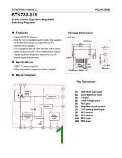
Thick Film Hybrid IC
INCHANGE
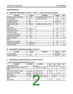
Specifications
Maximum Ratings at Ta=25℃, Tc=25℃ unless otherwise specified
Parameter
Operating substrate temperature
AC input voltage
Symbol
TC max
VAC
Conditions
Recommended value is 105℃
Specified test circuit
Ratings
115
UNIT
℃
140
Vrms
℃
Operating temperature
Storage temperature
Maximum output power
(TR1)
Topr
-10 to+85
-30 to+115
110
Tstg
℃
Wo max
Specified test circuit VO=135V
W
Drain current
6
20
A
A
ID
ID(Pulse)
IDR
Pulse drain current
Drain reverse current
Gate-source voltage
Allowable power dissipation
Chip junction temperature
Thermal resistance
(ZD1)
6
A
±30
78.1
150
1.6
V
VGSS
PD
W
Tj max
θj-c
℃
℃/W
Allowable power dissipation
Chip junction temperature
Thermal resistance
500
125
0.2
mW
℃
PZD1
Tj(ZD1)max
θj-c(ZD1)
℃/mW
Allowable operating ranges at Ta=25℃
Parameter
Pin 4 input voltage
Oscillator frequency
Symbol
V4
Conditions
Ratings
±8 to±24
20 to 120
UNIT
V
fOSC
kHz
Operating characteristics at Ta=25℃Tc=25℃
( unless otherwise specified,specified test circuits)
Parameter
Output voltage setting
Symbol
Conditions
IIN=8mA
min
Typ
max
UNIT
V
40.0
40.5
7
41.0
Output voltage temperature coefficient
(TR1)
mV/℃
TC=0 to 105℃, IIN=8mA
Drain-source breakdown voltage
Gate-source cutoff voltage
ON resistance
500
2.0
V
V
V(BR)DSS
VGS(off)
RDS(on)
Ciss
ID=10mA,VGS=0V
3.0
1.8
ID=1mA,VDS=10V
1.4
Ω
pF
ID=2.5A,VGS=10V
Input capacitance
(ZD1)
800
VDS=10V,VGS=0V,f=1MHz
Zener voltage
23.7
26.3
V
VZ
IZ=5mA

 ISC [ INCHANGE SEMICONDUCTOR COMPANY LIMITED ]