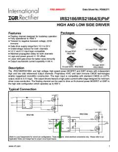
IRS2186/IRS21864(S)PbF
PRELIMINARY
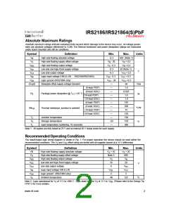
Absolute Maximum Ratings
Absolute maximum ratings indicate sustained limits beyond which damage to the device may occur. All voltage param-
eters are absolute voltages referenced to COM. The thermal resistance and power dissipation ratings are measured
under board mounted and still air conditions.
Symbol
Definition
High side floating absolute voltage
High side floating supply offset voltage
High side floating output voltage
Min.
Max.
Units
V
-0.3
620 (Note 1)
B
S
V
V
- 20
V
+ 0.3
+ 0.3
B
S
B
V
HO
V
- 0.3
V
B
V
Low side and logic fixed supply voltage
Low side output voltage
-0.3
-0.3
- 0.3
20 (Note 1)
CC
V
V
LO
V
+ 0.3
+ 0.3
CC
V
Logic input voltage (HIN & LIN - IRS2186/IRS21864)
Logic ground (IRS21864 only)
V
V
CC
IN
SS
V
SS
V
- 20
V
CC
+ 0.3
CC
dV /dt
Allowable offset supply voltage transient
—
50
V/ns
W
S
(8-lead PDIP)
—
1.0
(8-lead SOIC)
(14-lead PDIP)
(14-lead SOIC)
(8-lead PDIP)
(8-lead SOIC)
(14-lead PDIP)
(14-lead SOIC)
—
—
—
—
—
—
—
—
0.625
1.6
P
D
Package power dissipation @ T ≤ +25 °C
A
1.0
125
200
75
°C/W
°C
Rth
Thermal resistance, junction to ambient
JA
120
150
150
300
T
J
Junction temperature
T
S
T
L
Storage temperature
-50
—
Lead temperature (soldering, 10 seconds)
Note 1: All suplies are fully tested at 25 V and an internal 20 V clamp exists for each supply.
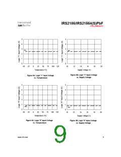
Recommended Operating Conditions
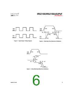
The Input/Output logic timing diagram is shown in Fig. 1. For proper operation the device should be used within the
recommended conditions. The V and V offset rating are tested with all supplies biased at a 15 V differential.
S
SS
Symbol
Definition
Min.
Max.
Units
VB
High side floating supply absolute voltage
High side floating supply offset voltage
High side floating output voltage
Low side and logic fixed supply voltage
Low side output voltage
V
+ 10
V + 20
S
S
V
S
Note 2
600
V
HO
V
S
V
B
V
CC
10
0
20
V
V
LO
V
CC
V
Logic input voltage HIN & LIN
Logic ground (IRS21864 only)
Ambient temperature
V
V
IN
SS
CC
V
SS
-5
5
T
A
-40
125
°C
Note 2: Logic operational for V of -5 V to +600 V. Logic state held for V of -5 V to -V . (Please refer to the Design Tip
S
S
BS
DT97-3 for more details).
www.irf.com
2

 INFINEON [ Infineon ]