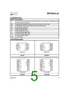
( )
S
( )
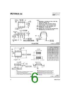
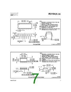
IR2184 4
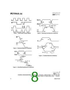
Dynamic Electrical Characteristics
V
(V , V ) = 15V, V = COM, C = 1000 pF, T = 25°C, DT = VSS unless otherwise specified.
BIAS CC BS
L
A
SS
Symbol
Definition
Min. Typ. Max. Units Test Conditions
t
t
t
Turn-on propagation delay
—
—
—
—
—
—
—
680
270
180
0
900
400
270
90
V = 0V
S
on
off
sd
Turn-off propagation delay
V
S
= 0V or 600V
Shut-down propagation delay
MTon
MToff
Delay matching, HS & LS turn-on
nsec
Delay matching, HS & LS turn-off
Turn-on rise time
0
40
t
t
40
20
60
V
V
= 0V
= 0V
r
S
Turn-off fall time
35
f
S
DT
Deadtime: LO turn-off to HO turn-on(DT
280
4
400
5
520
6
RDT= 0
RDT = 200k
RDT=0
LO-HO) &
HO turn-off to LO turn-on (DT
µsec
HO-LO)
HO-LO
MDT
Deadtime matching = DT
- DT
—
0
50
LO - HO
nsec
—
0
600
RDT = 200k
Static Electrical Characteristics
V
(V , V ) = 15V, V
CC BS
= COM, DT= V
and T = 25°C unless otherwise specified. The V , V and I
SS A IL IH IN
BIAS
SS
parameters are referenced to V /COM and are applicable to the respective input leads: IN and SD. The V , I and Ron
SS
O O
parameters are referenced to COM and are applicable to the respective output leads: HO and LO.
Symbol
Definition
Min. Typ. Max. Units Test Conditions
V
Logic “1” input voltage for HO & logic “0” for LO
2.7
—
—
—
—
—
—
—
60
1.0
5
—
0.8
—
V
V
V
V
= 10V to 20V
= 10V to 20V
= 10V to 20V
= 10V to 20V
IH
CC
CC
CC
CC
V
Logic “0” input voltage for HO & logic “1” for LO
—
IL
SD,TH+
V
SD input positive going threshold
SD input negative going threshold
2.7
—
V
V
0.8
1.2
0.1
50
SD,TH-
V
OH
High level output voltage, V
- V
O
—
—
I
I
= 0A
= 0A
BIAS
O
V
Low level output voltage, V
O
OL
LK
O
I
Offset supply leakage current
Quiescent V supply current
—
V = V = 600V
B S
µA
mA
µA
I
20
0.4
—
150
1.6
20
V
= 0V or 5V
= 0V or 5V
QBS
QCC
BS
IN
IN
I
Quiescent V
supply current
V
CC
I
Logic “1” input bias current
Logic “0” input bias current
IN = 5V, SD = 0V
IN = 0V, SD = 5V
IN+
I
—
1
2
IN-
V
V
CC
and V supply undervoltage positive going
8.0
8.9
9.8
CCUV+
BS
V
threshold
BSUV+
V
V
V
and V dupply undervoltage negative going
7.4
0.3
8.2
0.7
9.0
—
CCUV-
CC
BS
threshold
BSUV-
V
A
V
Hysteresis
CCUVH
V
BSUVH
I
Output high short circuit pulsed vurrent
Output low short circuit pulsed current
1.4
1.8
1.9
2.3
—
—
V = 0V,
O
O+
PW ≤ 10 µs
= 15V,
I
V
O
O-
PW ≤ 10 µs
www.irf.com
3

 INFINEON [ Infineon ]