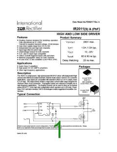
IR2011(S) & (PbF)
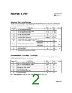
Absolute Maximum Ratings
Absolute maximum ratings indicate sustained limits beyond which damage to the device may occur. All voltage param-
eters are absolute voltages referenced to COM. The thermal resistance and power dissipation ratings are measured
under board mounted and still air conditions.
Symbol
Definition
Min.
Max.
Units
V
V
High side floating supply voltage
-0.3
250
B
S
High side floating supply offset voltage
High side floating output voltage
Low side fixed supply voltage
V
- 25
V
V
+ 0.3
+ 0.3
25
B
B
V
HO
V
CC
V
- 0.3
S
B
-0.3
-0.3
V
V
Low side output voltage
V
V
+0.3
+0.3
LO
CC
CC
V
IN
Logic input voltage (HIN & LIN)
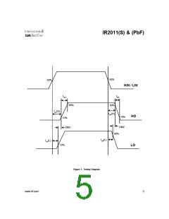
Allowable offset supply voltage transient (figure 2)
COM -0.3
dV /dt
s
—
—
—
—
—
—
-55
—
50
V/ns
W
P
Package power dissipation @ T ≤ +25°C
(8-lead DIP)
(8-lead SOIC)
(8-lead DIP)
(8-lead SOIC)
1.0
0.625
125
200
150
150
300
D
A
R
Thermal resistance, junction to ambient
THJA
°C/W
°C
T
T
Junction temperature
J
Storage temperature
S
T
Lead temperature (soldering, 10 seconds)
L
Recommended Operating Conditions
For proper operation the device should be used within the recommended conditions. The V and COM offset ratings
S
are tested with all supplies biased at 15V differential.
Symbol
Definition
High side floating supply absolute voltage
High side floating supply offset voltage
High side floating output voltage
Low side fixed supply voltage
Low side output voltage
Min.
Max.
Units
V
V
V
S
+ 10
V + 20
S
B
S
Note 1
200
V
HO
V
CC
V
V
B
S
V
10
0
20
VCC
5.5
V
LO
V
Logic input voltage (HIN & LIN)
Ambient temperature
COM
-40
IN
T
A
125
°C
Note 1: Logic operational for V of -4 to +200V. Logic state held for V of -4V to -V .
BS
S
S
2
www.irf.com

 INFINEON [ Infineon ]