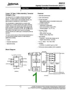
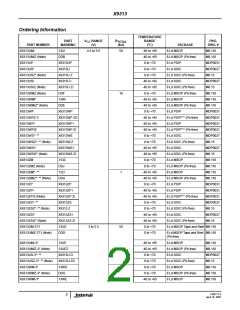
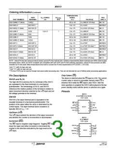
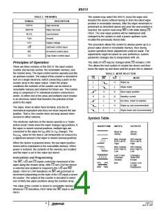
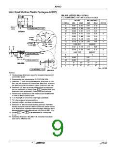
X9313
Absolute Maximum Ratings
Recommended Operating Conditions
Temperature Under Bias . . . . . . . . . . . . . . . . . . . . .-65°C to +135°C
Storage Temperature . . . . . . . . . . . . . . . . . . . . . . . .-65°C to +150°C
Voltage on CS, INC, U/D, and
Temperature:
Commercial. . . . . . . . . . . . . . . . . . . . . . . . . . . . . . . . 0°C to +70°C
Industrial . . . . . . . . . . . . . . . . . . . . . . . . . . . . . . . . .-40°C to +85°C
Supply Voltage (VCC):
X9313 . . . . . . . . . . . . . . . . . . . . . . . . . . . . . . . . . . . . . . . .5V ±10%
X9313-3 . . . . . . . . . . . . . . . . . . . . . . . . . . . . . . . . . . . . 3V to 5.5V
Max Wiper current . . . . . . . . . . . . . . . . . . . . . . . . . . . . . . . . .±4.4mA
Power rating:
V
with respect to V . . . . . . . . . . . . . . . . . . . . . . . . -1V to +7V
SS
CC
Voltage on V , V , V
W
H
L
with respect to V . . . . . . . . . . . . . . . . . . . . . . . . . . . . -6V to +7V
SS
ΔV = |V - V |:
H
L
X9313Z . . . . . . . . . . . . . . . . . . . . . . . . . . . . . . . . . . . . . . . . . . . .4V
X9313W, X9313U . . . . . . . . . . . . . . . . . . . . . . . . . . . . . . . . . . .10V
Lead Temperature (soldering 10s). . . . . . . . . . . . . . . . . . . . .+300°C
R
R
≥ 10kΩ . . . . . . . . . . . . . . . . . . . . . . . . . . . . . . . . . . . .10mW
1kΩ. . . . . . . . . . . . . . . . . . . . . . . . . . . . . . . . . . . . . . .16mW
TOTAL
TOTAL
I
(10s) . . . . . . . . . . . . . . . . . . . . . . . . . . . . . . . . . . . . . . . . .±8.8mA
Pb-free reflow profile . . . . . . . . . . . . . . . . . . . . . . . . . .see link below
http://www.intersil.com/pbfree/Pb-FreeReflow.asp
Pb-free PDIPs can be used for through hole wave solder processing
only. They are not intended for use in Reflow solder processing
applications
W
ESD Rating
Human Body Model (Per MIL-STD-883 Method 3015.7) . . . 2.0kV
Machine Model (Per EIAJ ED-4701 Method C-111). . . . . . . .200V
CAUTION: Stresses above those listed under “Absolute Maximum Ratings” may cause permanent damage to the device. This is a stress rating only; functional
operation of the device (at these or any other conditions above those listed in the operational sections of this specification) is not implied. Exposure to absolute
maximum rating conditions for extended periods may affect device reliability.
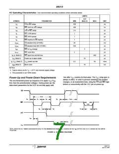
Potentiometer CharacteristicsOver recommended operating conditions unless otherwise stated.
LIMITS
SYMBOL
PARAMETER
TEST CONDITIONS/NOTES
MIN
TYP
MAX
UNIT
%
End-to-end resistance tolerance
±20
V
V
V
terminal voltage
terminal voltage
-V
+V
CC
V
VH
H
L
CC
V
-V
+V
CC
V
VL
CC
R
Wiper resistance
Wiper current
I
= (V - V )/R
, V
= 5V
40
100
Ω
W
W
H
L
TOTAL CC
I
±4.4
mA
dBV
%
W
Noise (Note 5)
Ref: 1kHz
-120
3
Resolution
Absolute linearity (Note 1)
R
R
- R
±1
MI
(Note 3)
W(n)(actual)
W(n)(expected)
Relative linearity (Note 2)
- (R
+MI)
±0.2
MI
W(n+1)
W(n)
(Note 3)
R
temperature coefficient (Note 5)
±300
±20
ppm/°C
ppm/°C
TOTAL
Ratiometric temperature coefficient
(Note 5)
C /C /C
W
Potentiometer capacitances
See Circuit #3
10/10/25
pF
H
L
(Note 5)
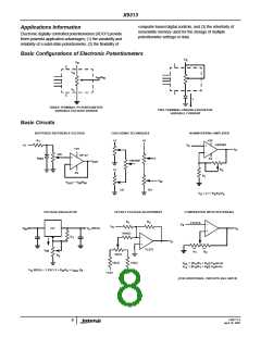
NOTES:
1. Absolute linearity is utilized to determine actual wiper voltage versus expected voltage = (V
- V
) = ±1 MI maximum.
W(n)(actual)
+ MI) = ±0.2 MI.
W(n)(expected)
2. Relative linearity is a measure of the error in step size between taps = R
W(n+1)
- (R
W(n)
3. 1 MI = minimum increment = R
/31.
TOT
FN8177.5
April 18, 2007
5

 INTERSIL [ Intersil ]