ISL88731A
Absolute Maximum Ratings
Thermal Information
DCIN, CSSP, CSSN, CSOP, CSON, VFB . . . . . . . . . .-0.3V to +28V
CSSP-CSSN, CSOP-CSON, PGND-GND. . . . . . . . . -0.3V to +0.3V
PHASE to GND . . . . . . . . . . . . . . . . . . . . . . . . . . . . . . . -6V to +30V
BOOT to GND . . . . . . . . . . . . . . . . . . . . . . . . . . . . . . .-0.3V to +33V
BOOT to PHASE . . . . . . . . . . . . . . . . . . . . . . . . . . . . . .-0.3V to +6V
UGATE . . . . . . . . . . . . . . . . . . . . . . .PHASE - 0.3V to BOOT +0.3V
LGATE . . . . . . . . . . . . . . . . . . . . . . . .PGND - 0.3V to VDDP +0.3V
ICOMP, VCOMP, VREF, to GND . . . . . . . . . . . . -0.3V to VCC +0.3V
VDDSMB, SCL, SDA, ACIN, ACOK . . . . . . . . . . . . . . .-0.3V to +6V
VDDP, ICM, VCC to GND, VDDP to PGND. . . . . . . . . .-0.3V to +6V
Thermal Resistance (Typical, Notes 1, 2)
θ
(°C/W)
39
θ
(°C/W)
9.5
JA
JC
QFN Package. . . . . . . . . . . . . . . . . . . .
Junction Temperature Range. . . . . . . . . . . . . . . . . .-55°C to +150°C
Operating Temperature Range . . . . . . . . . . . . . . . .-10°C to +100°C
Storage Temperature . . . . . . . . . . . . . . . . . . . . . . . .-65°C to +150°C
Pb-Free Reflow Profile. . . . . . . . . . . . . . . . . . . . . . . . .see link below
http://www.intersil.com/pbfree/Pb-FreeReflow.asp
CAUTION: Do not operate at or near the maximum ratings listed for extended periods of time. Exposure to such conditions may adversely impact product reliability and
result in failures not covered by warranty.
NOTES:
1. θ is measured with the component mounted on a highly effective thermal conductivity test board on free air. See Tech Brief TB379 for details.
JA
2. For θ , the “case temp” location is the center of the exposed metal pad on the package underside.
JC
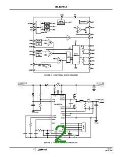
Electrical Specifications DCIN = CSSP = CSSN = 18V, CSOP = CSON = 12V, VDDP = 5V, BOOT-PHASE = 5.0V, GND = PGND = 0V,
CVDDP = 1µF, IVDDP = 0mA, T = -10°C to +100°C. Parameters with MIN and/or MAX limits are 100% tested
A
at +25°C, unless otherwise specified. Temperature limits established by characterization and are not production
tested.
PARAMETER
CONDITIONS
MIN
TYP
MAX
UNITS
CHARGE VOLTAGE REGULATION
Battery Full Charge Voltage and Accuracy ChargeVoltage = 0x41A0
16.716
-0.5
16.8
16.884
0.5
V
%
V
ChargeVoltage = 0x3130
12.529
-0.5
12.592
8.4
12.655
0.5
%
V
ChargeVoltage = 0x20D0
8.350
-0.6
8.450
0.6
%
V
ChargeVoltage = 0x1060
4.163
-0.7
4.192
4.221
0.7
%
V
Battery Undervoltage Lockout Trip Point
for Trickle Charge
VFB rising
2.55
2.7
2.85
Battery Undervoltage Lockout Trip Point
Hysteresis
100
250
400
mV
mV
CHARGE CURRENT REGULATION
CSOP to CSON Full-Scale Current-Sense
Voltage
78.22
80.64
8.064
83.06
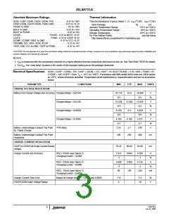
Charge Current and Accuracy
RS2 = 10mΩ (see Figure 2)
ChargingCurrent = 0x1f80
7.822
-3
8.306
3
A
%
RS2 = 10mΩ (see Figure 2)
ChargingCurrent = 0x0f80
3.809
-4
3.968
128
4.126
4
A
%
RS2 = 10mΩ (see Figure 2)
64
220
mA
ChargingCurrent = 0x0080
Charge Current Gain Error
Based on charge current = 128mA and 8.064A
-1.6
0
1.4
19
%
V
CSOP/CSON Input Voltage Range
FN6738.0
July 23, 2008
3

 INTERSIL [ Intersil ]