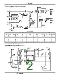
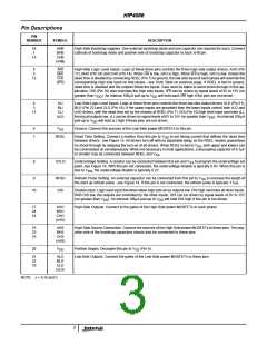
HIP4086
Pin Descriptions
PIN
NUMBER
SYMBOL
DESCRIPTION
16
1
13
AHB
BHB
CHB
(xHB)
High-Side Bootstrap supplies. One external bootstrap diode and one capacitor are required for each. Connect
cathode of bootstrap diode and positive side of bootstrap capacitor to each xHB pin.
5
2
12
AHI
BHI
CHI
(xHI)
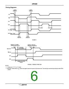
High-Side Logic Level Inputs. Logic at these three pins controls the three high side output drivers, AHO (Pin
17), BHO (Pin 24) and CHO (Pin 14). When xHI is low, xHO is high. When xHI is high, xHO is low. Unless the
dead time is disabled by connecting RDEL (Pin 7) to ground, the low side input of each phase will override the
corresponding high side input on that phase - see Truth Table on previous page. If RDEL is tied to ground,
dead time is disabled and the outputs follow the inputs. Care must be taken to avoid shoot-through in this ap-
plication. DIS (Pin 10) also overrides the high side inputs. xHI can be driven by signal levels of 0V to 15V (no
greater than V ). An internal 100µA pull-up to V
DD
will hold each xHI high if the pins are not driven.
DD
4
3
11
ALI
BLI
CLI
(xLI)
Low-Side Logic Level Inputs. Logic at these three pins controls the three low side output drivers ALO (Pin 21),
BLO (Pin 22) and CLO (Pin 19). If the upper inputs are grounded then the lower inputs control both xLO and
xHO drivers, with the dead time set by the resistor at RDEL (Pin 7). DIS (Pin 10) high level input overrides xLI,
forcing all outputs low. xLI can be driven by signal levels of 0V to 15V (no greater than V ). An internal 100µA
DD
pull-up to V
will hold xLI high if these pins are not driven.
DD
6
7
V
SS
Ground. Connect the sources of the Low-Side power MOSFETs to this pin.
RDEL
Dead Time Setting. Connect a resistor from this pin to V
to set timing current that defines the dead time
DD
between drivers - see Figure 15. All drivers turn-off with no adjustable delay, so the RDEL resistor guarantees
no shoot-through by delaying the turn-on of all drivers. When RDEL is tied to V , both upper and lowers can
SS
be commanded on simultaneously. While not necessary in most applications, a decoupling capacitor of 0.1µF
or smaller may be connected between RDEL and V
.
SS
8
UVLO
Undervoltage Setting. A resistor can be connected between this pin and V to program the undervoltage set
SS
point, see Figure 16. With this pin not connected, the undervoltage disable is typically 6.6V. When this pin is
tied to V , the undervoltage disable is typically 6.2V.
DD
9
RFSH
DIS
Refresh Pulse Setting. An external capacitor can be connected from this pin to V
the start up refresh pulse - see Figure 14. If this pin is not connected, the refresh pulse is typically 1.5µs.
to increase the length of
SS
10
Disable Input. Logic level input that when taken high sets all six outputs low. DIS high overrides all other inputs.
With DIS low, the outputs are controlled by the other inputs. DIS can be driven by signal levels of 0V to 15V
(no greater than V ). An internal 100µA pull-up to V
DD
will hold DIS high if this pin is not driven.
DD
17
24
14
AHO
BHO
CHO
(xHO)
High-Side Outputs. Connect to the gates of the High-Side power MOSFETs in each phase.
15
23
15
AHS
BHS
CHS
(xHS)
High-Side Source Connection. Connect the sources of the High-Side power MOSFETs to these pins. The neg-
ative side of the bootstrap capacitors should also be connected to these pins.
20
V
Positive Supply. Decouple this pin to V
(Pin 6).
DD
SS
21
22
19
ALO
BLO
CLO
(xLO)
Low-Side Outputs. Connect the gates of the Low-Side power MOSFETs to these pins.
NOTE: x = A, B and C.
3

 INTERSIL [ Intersil ]