EL7155
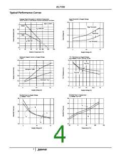
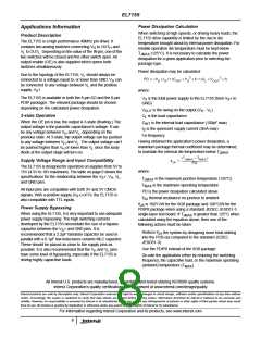
Power Dissipation Calculation
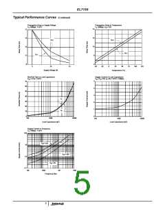
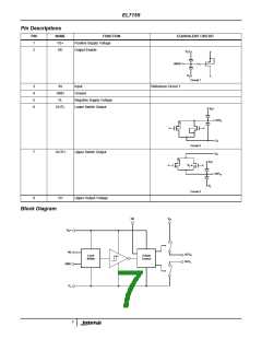
Applications Information
When switching at high speeds, or driving heavy loads, the
EL7155 drive capability is limited by the rise in die
temperature brought about by internal power dissipation. For
reliable operation die temperature must be kept below
Product Description
The EL7155 is a high performance 40MHz pin driver. It
contains two analog switches connecting V to OUT and
H
H
V to OUT . Depending on the value of the IN pin, one of the
L
L
T
(125°C). It is necessary to calculate the power
JMAX
two switches will be closed and the other switch open. An
output enable (OE) is also supplied which opens both
switches simultaneously.
dissipation for a given application prior to selecting the
package type.
Power dissipation may be calculated:
Due to the topology of the EL7155, V should always be
L
2
2
PD = (V × I ) + (C
× V × f) + (C × V
× f)
OUT
connected to a voltage equal to, or lower than GND. V can
H
S
S
INT
S
L
be connected to any voltage between V and the positive
L
supply, V +.
S
where:
The EL7155 is available in both the 8-pin SO and the 8-pin
PDIP packages. The relevant package should be chosen
depending on the calculated power dissipation.
V is the total power supply to the EL7155 (from V + to
GND)
S
S
V
is the swing on the output (V - V )
H L
OUT
C is the load capacitance
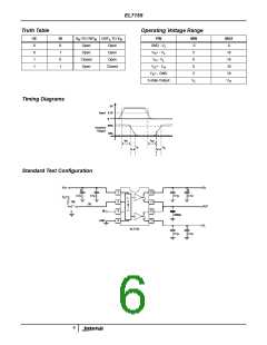
3-state Operation
L
When the OE pin is low, the output is 3-state (floating.) The
output voltage is the parasitic capacitance’s voltage. It can
C
is the internal load capacitance (100pF max)
INT
is the quiescent supply current (3mA max)
I
S
be any voltage between V and V , depending on the
H
L
f is frequency
previous state. At 3-state, the output voltage can be pushed
to any voltage between V and V . The output voltage can’t
Having obtained the application’s power dissipation, a
maximum package thermal coefficient may be determined,
to maintain the internal die temperature below T
H
L
be pushed higher than V or lower than V since the body
H
L
:
diode at the output stage will turn on.
JMAX
(T
– T
)
MAX
JMAX
Supply Voltage Range and Input Compatibility
θ
= ----------------------------------------------
JA
PD
The EL7155 is designed for operation on supplies from 5V to
15V (4.5V to 18V maximum). The table on page 6 shows the
where:
specifications for the relationship between the V +, V , V ,
and GND pins.
S
H
L
T
T
is the maximum junction temperature (125°C)
JMAX
is the maximum operating temperature
MAX
All input pins are compatible with both 3V and 5V CMOS
signals. With a positive supply (V +) of 5V, the EL7155 is
S
also compatible with TTL inputs.
PD is the power dissipation calculated above
θ
thermal resistance on junction to ambient
JA
is 160°C/W for the SO8 package and 100°C/W for the
θ
JA
Power Supply Bypassing
PDIP8 package when using a standard JEDEC JESD51-3
When using the EL7155, it is very important to use adequate
power supply bypassing. The high switching currents
developed by the EL7155 necessitate the use of a bypass
single-layer test board. If T is greater than 125°C when
calculated using the equation above, then one of the
following actions must be taken:
JMAX
capacitor between the V + and GND pins. It is
S
Reduce θ the system by designing more heat-sinking
into the PCB (as compared to the standard JEDEC
JESD51-3)
JA
recommended that a 2.2µF tantalum capacitor be used in
parallel with a 0.1µF low-inductance ceramic MLC capacitor.
These should be placed as close to the supply pins as
Use the PDIP8 instead of the SO8 package
possible. It is also recommended that the V and V pins
H
L
have some level of bypassing, especially if the EL7155 is
driving highly capacitive loads.
De-rate the application either by reducing the switching
frequency, the capacitive load, or the maximum operating
(ambient) temperature (T
)
MAX
All Intersil U.S. products are manufactured, assembled and tested utilizing ISO9000 quality systems.
Intersil Corporation’s quality certifications can be viewed at www.intersil.com/design/quality
Intersil products are sold by description only. Intersil Corporation reserves the right to make changes in circuit design, software and/or specifications at any time without
notice. Accordingly, the reader is cautioned to verify that data sheets are current before placing orders. Information furnished by Intersil is believed to be accurate and
reliable. However, no responsibility is assumed by Intersil or its subsidiaries for its use; nor for any infringements of patents or other rights of third parties which may result
from its use. No license is granted by implication or otherwise under any patent or patent rights of Intersil or its subsidiaries.
For information regarding Intersil Corporation and its products, see www.intersil.com
8

 INTERSIL [ Intersil ]