CA3146, CA3146A, CA3183, CA3183A
Absolute Maximum Ratings
Thermal Information
o
Collector-to-Emitter Voltage (V
)
Thermal Resistance (Typical, Note 2)
θJA ( C/W)
CEO
CA3146A, CA3183A. . . . . . . . . . . . . . . . . . . . . . . . . . . . . . . . . . 40V
CA3146, CA3183 . . . . . . . . . . . . . . . . . . . . . . . . . . . . . . . . . . . . 30V
14 Ld PDIP Package . . . . . . . . . . . . . . . . . . . . . . . .
14 Ld SOIC Package . . . . . . . . . . . . . . . . . . . . . . . .
16 Ld PDIP Package . . . . . . . . . . . . . . . . . . . . . . . .
16 Ld SOIC Package . . . . . . . . . . . . . . . . . . . . . . . .
Maximum Power Dissipation (Any One Transistor, Note 3)
CA3146A, CA3146. . . . . . . . . . . . . . . . . . . . . . . . . . . . . . . . 300mW
CA3183A, CA3183. . . . . . . . . . . . . . . . . . . . . . . . . . . . . . . . 500mW
Maximum Junction Temperature (Die). . . . . . . . . . . . . . . . . . . . 175 C
Maximum Junction Temperature (Plastic Package). . . . . . . . .150 C
Maximum Storage Temperature Range (all types) . -65 C to 150 C
Maximum Lead Temperature (Soldering 10s) . . . . . . . . . . . . .300 C
100
200
95
Collector-to-Base Voltage (V
)
CBO
CA3146A, CA3183A. . . . . . . . . . . . . . . . . . . . . . . . . . . . . . . . . . 50V
CA3146, CA3183 . . . . . . . . . . . . . . . . . . . . . . . . . . . . . . . . . . . . 40V
175
Collector-to-Substrate Voltage (V
, Note 1)
CIO
CA3146A, CA3183A. . . . . . . . . . . . . . . . . . . . . . . . . . . . . . . . . . 50V
CA3146, CA3183 . . . . . . . . . . . . . . . . . . . . . . . . . . . . . . . . . . . . 40V
o
o
Emitter to Base Voltage (V ) all types. . . . . . . . . . . . . . . . . . . . . 5V
EBO
o
o
Collector Current
CA3146A, CA3146 . . . . . . . . . . . . . . . . . . . . . . . . . . . . . . . . . 50mA
CA3183A, CA3183 . . . . . . . . . . . . . . . . . . . . . . . . . . . . . . . . . 75mA
o
(SOIC - Lead Tips Only)
Base Current (I ) - CA3183A, CA3183 . . . . . . . . . . . . . . . . . . . 20mA
B
Operating Conditions
o
o
Temperature Range . . . . . . . . . . . . . . . . . . . . . . . . . . -40 C to 85 C
CAUTION: Stresses above those listed in “Absolute Maximum Ratings” may cause permanent damage to the device. This is a stress only rating and operation of the
device at these or any other conditions above those indicated in the operational sections of this specification is not implied.
NOTES:
1. The collector of each transistor is isolated from the substrate by an integral diode. The substrate must be connected to a voltage which is more
negative than any collector voltage in order to maintain isolation between transistors, and to provide for normal transistor action. To avoid
undesired coupling between transistors, the substrate terminal should be maintained at either DC or signal (AC) ground. A suitable bypass
capacitor can be used to establish a signal ground.
2. θ is measured with the component mounted on an evaluation PC board in free air.
JA
3. Care must be taken to avoid exceeding the maximum junction temperature. Use the total power dissipation (all transistors) and thermal
resistances to calculate the junction temperature.
Electrical Specifications CA3146 Series
TEST CONDITIONS TYPICAL
PERF.
CA3146
TYP
CA3146A
TYP
CURVE
FIG. NO.
o
PARAMETER
SYMBOL
T
= 25 C
MN
MAX
MIN
MAX UNITS
A
DC CHARACTERISTICS FOR EACH TRANSISTOR
Collector-to-Base
Breakdown Voltage
V
V
I
I
= 10µA, I = 0
-
-
-
40
30
40
72
56
72
7
-
-
-
50
40
50
72
56
72
7
-
-
-
V
V
V
(BR)CBO
C
E
Collector-to-Emitter
Breakdown Voltage
= 1mA, I = 0
B
(BR)CEO
C
Collector-to-Substrate
Breakdown Voltage
V
I
I
= 10µA, I = 0,
(BR)CIO
CI
E
B
= 0
Emitter-to-Base Breakdown Voltage
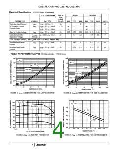
Collector-Cutoff Current
V
I
= 10µA, I = 0
-
5
-
-
5
-
-
V
(BR)EBO
E
C
I
I
V
= 10V, I = 0
1
See
Curve
5
See
Curve
5
µA
CEO
CE
B
Collector-Cutoff Current
V
V
V
V
V
= 10V, I = 0
2
3
3
3
4
5
-
0.002
85
100
-
0.002
85
100
nA
-
CBO
CB
CE
CE
CE
CE
E
DC Forward-Current Transfer
Ratio
h
= 5V, I = 10mA
-
30
-
-
-
30
-
-
FE
BE
C
= 5V, I = 1mA
100
90
-
100
90
-
-
C
= 5V, I = 10µA
-
0.83
-
-
0.83
-
-
C
Base-to-Emitter Voltage
V
= 3V, I = 1mA
0.63
-
0.73
0.33
0.63
-
0.73
0.33
V
V
C
Collector-to-Emitter
Saturation Voltage
V
I = 10mA, I = 1mA
C B
CE SAT
DC CHARACTERISTICS FOR TRANSISTORS Q AND Q (As A Differential Amplifier)
1
2
Magnitude of Input Offset
Voltage |V - V
|V
|
V
= 5V, I = 1mA
6, 7
-
-
0.48
1.9
5
-
-
-
0.48
1.9
5
-
mV
IO
CE
E
|
BE2
BE1
o
Magnitude of Base-to-Emitter
Temperature Coefficient
V
= 5V, I = 1mA
-
mV/ C
CE
E
∆V
BE
----------------
∆T
2

 INTERSIL [ Intersil ]