BUZ71A
o
Absolute Maximum Ratings
T = 25 C, Unless Otherwise Specified
C
BUZ71A
UNITS
Drain to Source Breakdown Voltage (Note 1) . . . . . . . . . . . . . . . . . . . . . . . . . . . . . . . . . . . . . V
50
50
V
V
DS
Drain to Gate Voltage (R
GS
= 20kΩ) (Note 1) . . . . . . . . . . . . . . . . . . . . . . . . . . . . . . . . . . . . V
DGR
o
Continuous Drain Current, T = 55 C . . . . . . . . . . . . . . . . . . . . . . . . . . . . . . . . . . . . . . . . . . . . . I
13
A
C
D
Pulsed Drain Current (Note 3) . . . . . . . . . . . . . . . . . . . . . . . . . . . . . . . . . . . . . . . . . . . . . . . . . .I
48
A
DM
Gate to Source Voltage . . . . . . . . . . . . . . . . . . . . . . . . . . . . . . . . . . . . . . . . . . . . . . . . . . . . . . V
±20
V
GS
Maximum Power Dissipation . . . . . . . . . . . . . . . . . . . . . . . . . . . . . . . . . . . . . . . . . . . . . . . . . . . P
40
W
mJ
D
Single Pulse Avalanche Energy Rating (Note 4) . . . . . . . . . . . . . . . . . . . . . . . . . . . . . . . . . . . E
100
AS
o
Linear Derating Factor . . . . . . . . . . . . . . . . . . . . . . . . . . . . . . . . . . . . . . . . . . . . . . . . . . . . . . . . . . .
0.32
-55 to 150
E
W/ C
o
Operating and Storage Temperature . . . . . . . . . . . . . . . . . . . . . . . . . . . . . . . . . . . . . . . . T , T
C
STG
J
DIN Humidity Category - DIN 40040 . . . . . . . . . . . . . . . . . . . . . . . . . . . . . . . . . . . . . . . . . . . . . . . .
IEC Climatic Category - DIN IEC 68-1. . . . . . . . . . . . . . . . . . . . . . . . . . . . . . . . . . . . . . . . . . . . . . .
Maximum Temperature for Soldering
55/150/56
o
Leads at 0.063in (1.6mm) from Case for 10s. . . . . . . . . . . . . . . . . . . . . . . . . . . . . . . . . . . . . .T
300
260
C
L
o
Package Body for 10s, See Techbrief 334 . . . . . . . . . . . . . . . . . . . . . . . . . . . . . . . . . . . . . . T
C
pkg
CAUTION: Stresses above those listed in “Absolute Maximum Ratings” may cause permanent damage to the device. This is a stress only rating and operation of the
device at these or any other conditions above those indicated in the operational sections of this specification is not implied.
NOTE:
o
o
1. T = 25 C to 125 C.
J
o
Electrical Specifications
PARAMETER
T = 25 C, Unless Otherwise Specified
C
SYMBOL
BV
TEST CONDITIONS
= 250µA, V = 0V
MIN
TYP
-
MAX
-
UNITS
V
Drain to Source Breakdown Voltage
Gate to Threshold Voltage
Zero Gate Voltage Drain Current
I
50
DSS
D
GS
V
V
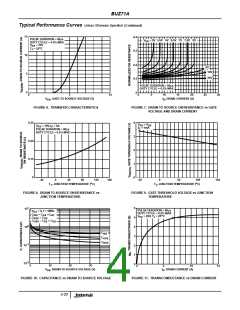
= V , I = 1mA (Figure 9)
2.1
3
4
V
GS(TH)
GS
DS
D
o
I
T = 25 C, V
J
= 50V, V = 0V
GS
-
20
250
1000
100
0.12
-
µA
µA
nA
Ω
DSS
DS
o
T = 125 C, V
= 50V, V
= 0V
= 0V
GS
-
100
10
J
DS
DS
Gate to Source Leakage Current
I
V
= 20V, V
-
GSS
GS
Drain to Source On Resistance (Note 2)
Forward Transconductance (Note 2)
Turn-On Delay Time
r
I
= 9A, V
= 10V (Figure 8)
-
0.11
5.2
20
DS(ON)
D
GS
g
V
= 25V, I = 9A (Figure 11)
3.0
S
DS
CC
D
fs
t
V
= 30V, ID ≈ 3A, V
GS
= 10V, R
= 50Ω,
GS
-
-
-
-
-
-
-
30
ns
ns
ns
ns
pF
pF
pF
d(ON)
R
= 10Ω
L
Rise Time
t
55
85
r
Turn-Off Delay Time
t
70
90
d(OFF)
Fall Time
t
80
110
650
450
280
f
Input Capacitance
C
V
= 25V, V = 0V, f = 1MHz (Figure 10)
GS
480
280
160
≤ 3.1
≤ 75
ISS
DS
Output Capacitance
C
OSS
RSS
Reverse Transfer Capacitance
Thermal Resistance Junction to Case
Thermal Resistance Junction to Ambient
C
o
R
C/W
θJC
θJA
o
R
C/W
Source to Drain Diode Specifications
PARAMETER
Continuous Source to Drain Current
Pulsed Source to Drain Current
Source to Drain Diode Voltage
Reverse Recovery Time
SYMBOL
TEST CONDITIONS
MIN
TYP
-
MAX
13
52
2.2
-
UNITS
o
I
T
T
= 25 C
-
-
-
-
-
A
A
SD
C
C
o
I
= 25 C
-
SDM
o
V
T = 25 C, I
J
= 26A, V
GS
= 0V, (Figure 12)
1.6
120
0.15
V
SD
SD
SD
o
t
T = 25 C, I
= 13, dI /dt = 100A/µs,
SD
ns
µC
rr
J
V
= 30V
R
Reverse Recovery Charge
NOTES:
Q
-
RR
2. Pulse Test: Pulse width ≤ 300µs, duty cycle ≤ 2%.
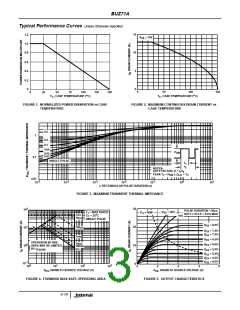
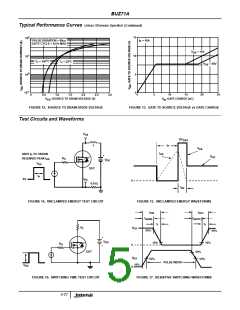
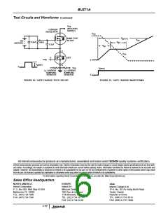
3. Repetitive rating: pulse width limited by maximum junction temperature. See Transient Thermal Impedance curve (Figure 3).
o
4. V
= 10V, T = 25 C, L = 820µH, I
= 14A. (See Figures 14 and 15).
PEAK
DD
J
4-18

 INTERSIL [ Intersil ]