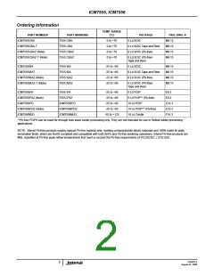
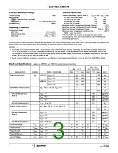
ICM7555, ICM7556
t
= -ln (1/3) R C = 1.1R C
V
OUTPUT
A
A
DD
R
R
V
A
B
DD
R
A
1
2
3
4
8
7
6
5
1
2
3
4
8
7
6
5
DISCHARGE
THRESHOLD
TRIGGER
OUTPUT
OUTPUT
ICM7555
CONTROL
VOLTAGE
V
DD
RESET
OPTIONAL
CAPACITOR
OPTIONAL
CAPACITOR
C
C
V
≤18V
DD
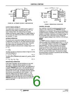
FIGURE 2B. ALTERNATE ASTABLE CONFIGURATION
FIGURE 3. MONOSTABLE OPERATION
CONTROL VOLTAGE
OUTPUT DRIVE CAPABILITY
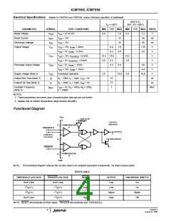
The CONTROL VOLTAGE terminal permits the two trip
voltages for the THRESHOLD and TRIGGER internal
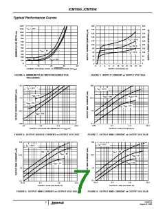
The output driver consists of a CMOS inverter capable of
driving most logic families including CMOS and TTL. As
such, if driving CMOS, the output swing at all supply
voltages will equal the supply voltage. At a supply voltage of
4.5V or more, the ICM7555 and ICM7556 will drive at least
two standard TTL loads.
comparators to be controlled. This provides the possibility of
oscillation frequency modulation in the astable mode or even
inhibition of oscillation, depending on the applied voltage. In
the monostable mode, delay times can be changed by
varying the applied voltage to the CONTROL VOLTAGE pin.
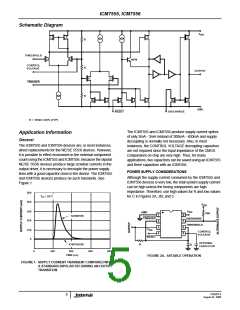
ASTABLE OPERATION
RESET
The circuit can be connected to trigger itself and free run as
a multivibrator, see Figure 2A. The output swings from rail to
rail, and is a true 50% duty cycle square wave. (Trip points
and output swings are symmetrical.) Less than a 1%
frequency variation is observed over a voltage range of +5V
to +15V.
The RESET terminal is designed to have essentially the
same trip voltage as the standard bipolar 555/6, i.e., 0.6V to
0.7V. At all supply voltages it represents an extremely high
input impedance. The mode of operation of the RESET
function is, however, much improved over the standard
bipolar NE/SE 555/6 in that it controls only the internal flip-
flop, which in turn controls simultaneously the state of the
OUTPUT and DISCHARGE pins. This avoids the multiple
threshold problems sometimes encountered with slow falling
edges in the bipolar devices.
1
------------------
f =
(EQ. 1)
1.4 RC
The timer can also be connected as shown in Figure 2B. In this
circuit, the frequency is:
(EQ. 2)
f = 1.44 ⁄ (R + 2R )C
A
B
The duty cycle is controlled by the values of R and R , by the
A
B
equation:
(EQ. 3)
D = (R + R ) ⁄ (R + 2R
)
A
B
A
B
MONOSTABLE OPERATION
In this mode of operation, the timer functions as a one-shot.
See Figure 3. Initially the external capacitor (C) is held
discharged by a transistor inside the timer. Upon application of
a negative TRIGGER pulse to pin 2, the internal flip-flop is set
which releases the short circuit across the external capacitor
and drives the OUTPUT high. The voltage across the capacitor
now increases exponentially with a time constant t = R C.
A
2
When the voltage across the capacitor equals / V+, the
3
comparator resets the flip-flop, which in turn discharges the
capacitor rapidly and also drives the OUTPUT to its low state.
TRIGGER must return to a high state before the OUTPUT can
return to a low state.
FN2867.9
August 24, 2006
6

 INTERSIL [ Intersil ]