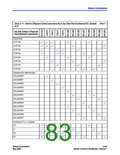
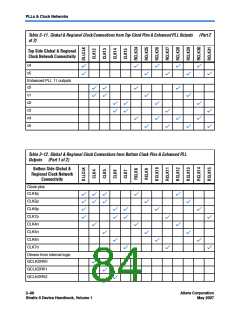
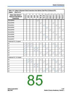
Stratix II Architecture
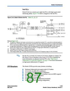
Fast PLLs
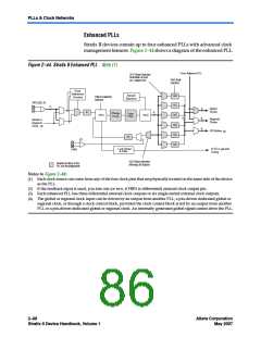
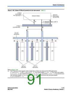
Stratix II devices contain up to eight fast PLLs with high-speed serial
interfacing ability. Figure 2–45 shows a diagram of the fast PLL.
Figure 2–45. Stratix II Device Fast PLL Notes (1), (2), (3)
Post-Scale
Counters
VCO Phase Selection
Selectable at each PLL
Output Port
Clock
Switchover
Circuitry (4)
Phase
Frequency
Detector
diffioclk0 (2)
Global or
regional clock (1)
load_en0
(3)
÷c0
÷c1
÷c2
(5)
8
Charge
Pump
(3)
(2)
Loop
Filter
load_en1
diffioclk1
÷k
÷n
PFD
VCO
4
Clock
Input
4
8
Global clocks
4
Global or
regional clock (1)
Regional clocks
÷c3
÷m
8
to DPA block
Shaded Portions of the
PLL are Reconfigurable
Notes to Figure 2–45:
(1) The global or regional clock input can be driven by an output from another PLL, a pin-driven dedicated global or
regional clock, or through a clock control block, provided the clock control block is fed by an output from another
PLL or a pin-driven dedicated global or regional clock. An internally generated global signal cannot drive the PLL.
(2) In high-speed differential I/O support mode, this high-speed PLL clock feeds the SERDES circuitry. Stratix II
devices only support one rate of data transfer per fast PLL in high-speed differential I/O support mode.
(3) This signal is a differential I/O SERDES control signal.
(4) Stratix II fast PLLs only support manual clock switchover.
(5) If the design enables this ÷2 counter, then the device can use a VCO frequency range of 150 to 520 MHz.
f
See the PLLs in Stratix II & Stratix II GX Devices chapter in volume 2 of
the Stratix II Device Handbook or the Stratix II GX Device Handbook for
more information on enhanced and fast PLLs. See “High-Speed
Differential I/O with DPA Support” on page 2–96 for more information
on high-speed differential I/O support.
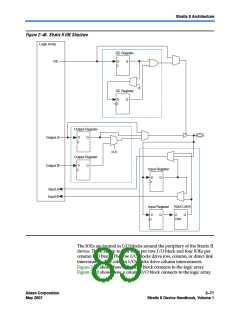
The Stratix II IOEs provide many features, including:
I/O Structure
■
■
■
■
■
■
■
■
Dedicated differential and single-ended I/O buffers
3.3-V, 64-bit, 66-MHz PCI compliance
3.3-V, 64-bit, 133-MHz PCI-X 1.0 compliance
Joint Test Action Group (JTAG) boundary-scan test (BST) support
On-chip driver series termination
On-chip parallel termination
On-chip termination for differential standards
Programmable pull-up during configuration
Altera Corporation
May 2007
2–69
Stratix II Device Handbook, Volume 1

 INTEL [ INTEL ]