®
MOBILE PENTIUM PROCESSOR WITH MMX™ TECHNOLOGY
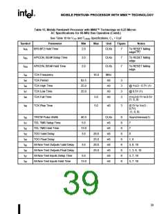
NOTES for TABLES 15 and 16:
®
Notes 2, 6, and 14 are general and apply to all standard TTL signals used with the Pentium processor family.
1. Not 100% tested. Guaranteed by design/characterization.
2. TTL input test waveforms are assumed to be 0 to 2.5V transitions with 1V/nS rise and fall times.
3. Non-test outputs and inputs are the normal output or input signals (besides TCK, TRST#, TDI, TDO, and TMS). These
timings correspond to the response of these signals due to boundary scan operations.
4. APCHK#, FERR#, HLDA, IERR#, LOCK#, and PCHK# are glitch-free outputs. Glitch-free signals monotonically transition
without false transitions (i.e., glitches).
5. 0.87V/ns £ CLK input rise/fall time £ 8.7V/ns.
6. 0.3V/ns £ input rise/fall time £ 5V/ns.
7. Referenced to TCK rising edge.
8. Referenced to TCK falling edge.
9. 1 ns can be added to the maximum TCK rise and fall times for every 10 MHz of frequency below 33 MHz.
10. During probe mode operation, do not use the boundary scan timings (t
11. Setup time is required to guarantee recognition on a specific clock.
12. Hold time is required to guarantee recognition on a specific clock.
13. All TTL timings are referenced from V CC3/2.
).
55-58
14. To guarantee proper asynchronous recognition, the signal must have been de-asserted (inactive) for a minimum of 2
clocks before being returned active and must meet the minimum pulse width.
15. This input may be driven asynchronously.
16. When driven asynchronously, RESET, NMI, FLUSH#, R/S#, INIT, and SMI# must be de-asserted (inactive) for a
minimum of 2 clocks before being returned active.
17. The D/C#, M/IO#, W/R#, CACHE#, and A5-A31 signals are sampled only on the CLK that ADS# is active.
18. BF[2:0] must not change values while RESET is active. In order to override the internal defaults and guarantee that the
BF[2:0] inputs remain stable while RESET is active, these pins should be strapped directly to or through a
pullup/pulldown resistor to VCC3 or ground. Driving these pins with active logic is not recommended unless stability
during RESET can be guaranteed.
19. These signals are measured on the rising edge of adjacent CLKs at V CC3/2. To ensure a 1:1 relationship between the
amplitude of the input jitter and the internal and external clocks, the jitter frequency spectrum should not have any power
spectrum peaking between 500 KHz and 1/3 of the CLK operating frequency. The amount of jitter present must be
accounted for as a component of CLK skew between devices. The internal clock generator requires a constant frequency
CLK input to within ±250ps. Therefore, the CLK input cannot be changed dynamically.
20. Timing (t14) is required for external snooping (e.g., address setup to the CLK in which EADS# is sampled active).
21. This assumes an external pullup resistor to VCC and a lumped capacitive load. The pullup resistor must be between 300
ohms and 1k ohms, the capacitance must be between 20pF and 120pF, and the RC product must be between 6nS and
36nS.
22. The CLK to PICCLK ratio has to be an integer and the ratio (CLK/PICCLK) cannot be smaller than 4.
23. CLK input frequency must be either 33.33 MHz (+1 MHz) or 66.66 MHz (-1 MHz). Operations in the range between 33.33
MHz and 66.6 MHz is not supported.
*
Each valid delay is specified for a 0 pF load. The system designer should us e I/O buffer modeling to account for signal
flight time delays.
41

 INTEL [ INTEL ]