Registers
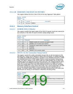
14.6.1.28 DDQSCADP1: DQS DELAY CAL PATTERN 1
This register defines the first 32 bits of the 64 bit long “aggressor” data pattern.
Device:
NodeID
Function: 4
Offset:
E0h
Bit
Attr
Default
Description
31:0
RW
db339ce1h ENABLE:
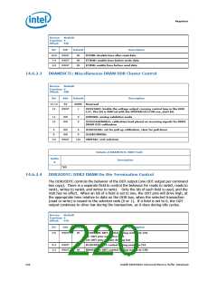
14.6.2
Memory Interface Control
14.6.2.1
DIOMON: DDR I/O Monitor
This register monitors the legsel output of the DDR I/O topcdat chunk and controls the
A/D converter in the DDR I/O used to monitor analog voltage levels.
Device:
NodeID
Function: 4
Offset:
Bit
F0h
Attr
Default
Description
15
14:12
11:8
7
RW
0
0h
0h
0h
0h
00h
ENABLE: Enable A/D converter and update vresult
BIASSEL: A/D converter input selection
LEGSELOUT: Legsel output of topcdat chunk
DIOPWR:
RWST
RWST
RWST
RV
6
Reserved
5:0
RWST
VRESULT: A/D converter output
14.6.2.2
ODTZTC: On-Die Termination Timing Control
This register controls the enable and disable timing of the on-die termination on DQ
and DQS pins. Timing can be adjusted in whole clock increments, or enabled statically.
The ETIMR and DTIMR fields are added in hardware to the SPDPAR13CUR.ODTZ_ETIMR
and SPDPAR13CUR.ODTZ_DTIMR register fields to control termination timing during
reads. The DRRTC register is also used to align the enable/disable time to when read
DQ/DQS signals are expected to arrive at the input pins. The combined default values
of the ODTZTC and SPDPAR13CUR fields enable termination 1/2 DRAM clock cycle
before the leading edge of the read DQS preamble arrives at the DQS pin, and keeps
termination enabled for 5 clock cycles in BL4 mode, and 7 cycles in BL8 mode. The DDR
I/O circuits automatically disable on-die termination when the DQ/DQS pins are
driving. The default register values enable termination during writes at the same time
that the pins are driving, so termination is effectively off during writes.
Device:
NodeID
Function: 4
Offset:
F4h
Bit
Attr
Default
Description
15
RWST
0
TIMORIDE: timing override. On-Die termination always on during read
operations and when the bus is idle
14:12
11
RWST
RV
0h
0
DTIMW: disable time after write data
Reserved
Intel® 6400/6402 Advanced Memory Buffer Datasheet
219

 INTEL [ INTEL ]