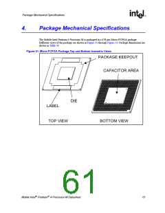
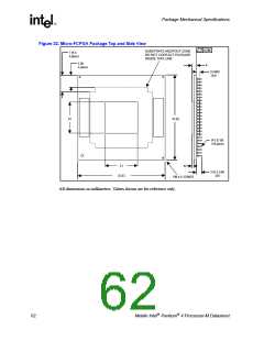
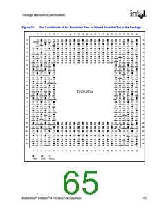
Package Mechanical Specifications
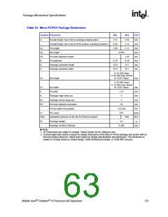
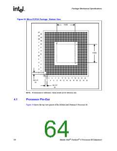
Table 34. Micro-FCPGA Package Dimensions
Symbol Parameter
Min
Max
Unit
A
Overall height, top of die to package seating plane
1.81
4.69
1.95
2.03
5.15
2.11
mm
mm
mm
mm
mm
mm
mm
mm
-
Overall height, top of die to PCB surface, including socket(1)
A1
A2
A3
B
Pin length
Die height
0.854
Pin-side capacitor height
Pin diameter
-
1.25
0.36
35.1
35.1
0.28
34.9
34.9
D
Package substrate length
Package substrate width
E
12.24 (B0 Step)
11.62 (B0 Step Shrink
& C1/D1 Step)
D1
Die length
mm
11.93 (B0 Step)
11.34 (B0 Step Shrink
& C1/D1 Step)
E1
e
Die width
mm
mm
mm
mm
mm
mm
each
kPa
g
Pin pitch
1.27
K
Package edge keep-out
Package corner keep-out
Pin-side capacitor boundary
Pin tip radial true position
Pin count
5
7
K1
K3
-
14
<=0.254
478
N
Pdie
W
Allowable pressure on the die for thermal solution
Package weight
-
689
4.5
Package Surface Flatness
0.286
mm
NOTES:
1. All Dimensions are subject to change. Values shown are for reference only.
2. Overall height with socket is based on design dimensions of the Micro-FCPGA package and socket with no
thermal solution attached. Values were based on design specifications and tolerances. This dimension is
subject to change based on socket design, OEM motherboard design, or OEM SMT process.
Mobile Intel Pentium 4 Processor-M Datasheet
63

 INTEL [ INTEL ]