Integrated T1 LH/SH Transceiver for DS1/DSX-1 or PRI Applications — LXT362
Tables
1
2
3
4
5
6
7
8
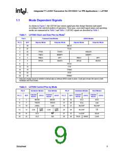
LXT362 Clock and Data Pins by Mode1 ...............................................................9
LXT362 Control Pins by Mode ..............................................................................9
LXT362 Signal Descriptions................................................................................10
CLKE Pin Settings1.............................................................................................18
Control and Operational Mode Selection ............................................................19
Diagnostic Mode Availability................................................................................20
Register Addresses.............................................................................................29
Register and Bit Summary ..................................................................................29
Control Register #1 Read/Write, Address (A7-A0) = x010000x..........................30
Equalizer Control Input Settings..........................................................................30
Control Register #2 Read/Write, Address (A7-A0) = x010001x..........................31
Control Register #3 Read/Write, Address (A7-A0) = x010010x..........................31
Interrupt Clear Register Read/Write, Address (A7-A0) = x010011x....................32
Transition Status Register Read Only, Address (A7-A0) = x010100x.................32
Performance Status Register Read Only, Address (A7-A0) = x010101x............33
Equalizer Status Register Read Only, Address (A7-A0) = x010110x .................33
Control Register #4 Read/Write, Address (A7-A0) = x010111x..........................33
Transmit Return Loss..........................................................................................34
Transformer Specifications for LXT362...............................................................34
Recommended Transformers for LXT362...........................................................35
Absolute Maximum Ratings.................................................................................38
Recommended Operating Conditions .................................................................38
Digital Characteristics..........................................................................................39
Analog Characteristics ........................................................................................39
1.544 MHz T1 Pulse Mask Corner Point Specifications......................................40
Master and Transmit Clock Timing Characteristics (See Figure 15)...................40
Receive Timing Characteristics (See Figure 16).................................................41
Serial I/O Timing Characteristics (See Figure 17 and Figure 18)........................42
9
10
11
12
13
14
15
16
17
18
19
20
21
22
23
24
25
26
27
28
Datasheet
5

 INTEL [ INTEL ]