TDA 5210
Applications
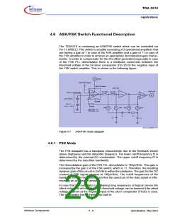
4.6 ASK/FSK Switch Functional Description
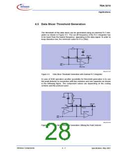
The TDA5210 is containing an ASK/FSK switch which can be controlled via
Pin 15 (MSEL). This switch is actually consisting of 2 operational amplifiers that
are having a gain of 1 in case of the ASK amplifier and a gain of 11 in case of
the FSK amplifier in order to achieve an appropriate demodulation gain charac-
teristic. In order to compensate for the DC-offset generated especially in case
of the FSK PLL demodulator there is a feedback connection between the
threshold voltage of the bit slicer comparator (Pin 20) to the negative input of
the FSK switch amplifier. This is shown in the following figure.
MSEL
15
RSSI (ASK signal)
ASK/FSK Switch
Data Filter
R2=100k
DATA Out
25
R1=100k
-
FSK PLL Demodulator
ASK
FSK
+
+
-
v = 1
Comp
+
-
0.18 mV/kHz
R3=300k
typ. 2 V
1.5 V......2.5 V
R4=30k
FFB
OPP SLP
SLN
22
21
19
20
ASK mode : v=1
FSK mode : v=11
R
C1
C2
C
ask_fsk_datapath.WMF
Figure 4-7
ASK/FSK mode datapath
4.6.1 FSK Mode
The FSK datapath has a bandpass characterisitc due to the feedback shown
above (highpass) and the data filter (lowpass). The lower cutoff frequency f2 is
determined by the external RC-combination. The upper cutoff frequency f3 is
determined by the data filter bandwidth.
The demodulation gain of the FSK PLL demodulator is 140µV/kHz. This gain is
increased by the gain v of the FSK switch, which is 11. Therefore the resulting
dynamic gain of this circuit is 2mV/kHz within the bandpass. The gain for the DC
content of FSK signal remains at 140µV/kHz. The cutoff frequencies of the
bandpass have to be chosen such that the spectrum of the data signal is influ-
enced in an acceptable amount.
In case that the user data is containing long sequences of logical zeroes the
effect of the drift-off of the bit slicer threshold voltage can be lowered if the offset
voltage inherent at the negative input of the slicer comparator (Pin20) is used.
The comparator has no hysteresis built in.
Wireless Components
4 - 8
Specification, May 2001

 INFINEON [ Infineon ]