TDA 4700
TDA 4718
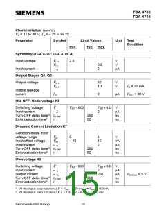
Characteristics (cont’d)
VS = 11 to 30 V; TA = – 25 to 85 °C
Parameter
Symbol
Limit Values
typ. max.
Unit Test
Condition
min.
Symmetry (TDA 4700; TDA 4700 A)
Input voltage
VI H
VI L
– II
2.0
V
V
µA
0.8
2
Input current
Output Stages Q1, Q2
Output voltage
VQ H
VQ L
30
1.1
V
V
IQ = 20 mA
Output leakage
current
IQ
2
µA
V
Q H = 30 V
ON, OFF, Undervoltage K6
Switching voltage
Input current
V
– II
VREF – 0.03
V
2
REF + 0.03 V
µA
ns
ns
Turn-OFF delay time1) tD OFF
250
50
Error detection time1)
t
Dynamic Current Limitation K7
Common-mode input
voltage range
VIC
VIO
– II
0
– 10
4
10
2
V
Input offset voltage
Input current
mV
µA
ns
ns
Turn-OFF delay time2) tD OFF
250
50
Error detection time2)
t
Overvoltage K5
Switching voltage
Input current
V
– II
– IQ
V
REF – 0.03
V
2
200
REF + 0.03 V
µA
µA
ns
ns
Output current
0
V
QH min = 5 V
Turn-OFF delay time1) tD OFF
250
50
Error detection time1)
t
1)
At the input: step function ∆V = VREF – 100 mV
V
REF + 100 mV
2)
At the input: step function ∆V = – 100 mV
∆V = + 100 mV
Semiconductor Group
15

 INFINEON [ Infineon ]