TC39x BC/BD-Step
HistoryChanges from Version 0.4 to Version 0.6
–
–
–
–
–
Change note of tRF from '0.5+0.075*CL ns' to '0.5+0.08*CL ns'
Change max value of tRF from 0.5+0.15*CL ns to 1.0+0.17*CL ns
Change note of tRF from '4+0.95*CL ns' to '12+1.0*CL ns'
Change max value of tRF from 2.5+0.35*CL ns to 5.0+0.35*CL ns
Change note of tRF from 'CL = 25pF; driver = strong sharp edge' to 'CL = 25pF; driver = strong sharp edge;
from 0.2 * VEXT/FLEX to 0.8 * VEXT/FLEX
'
–
–
–
Change note of fIND from '' to 'AL and TTL'
Change note of fOUTD from '' to 'medium driver'
Change note of IPDL from 'VIL; AL or TTL' to 'VIL; AL'
•
•
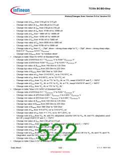
Changes in table 'Class D' of Standard Pads
–
–
Update footnote of Standard Pads to 'For AN11 200 nA need to be added.'
Change note of IOZ from 'TJ ≤ 150°C; PDD option available, or AltRef option available and EDSADC
channel connected' to 'TJ ≤ 150°C; PDD option available, or AltRef option available and EDSADC channel
connected, or two EDSADC channels connected'
Changes in table 'LVDS - IEEE standard LVDS general purpose link (GPL)' of LVDS Pads
–
–
–
–
Change max value of trise20 from 0.5 ns to 0.75 ns
Change max value of tfall20 from 0.5 ns to 0.75 ns
Change max value of VOD from 450 mV to 500 mV
Change min value of VOD from 360 mV to 380 mV
•
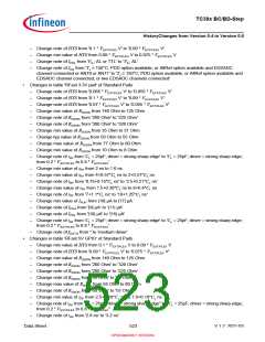
VADC 5V
–
–
–
–
–
–
Change max value of dVCSD from 20 % to 10 %
Change note of dVCSD from '-20 %' to '-10 %'
Change note of fADCI from 'Upper voltage range' to '4.5V ≤ VDDM ≤ 5.5V'
Change note of tSCAL from 'Upper voltage range' to '4.5V ≤ VDDM ≤ 5.5V'
Change note of fADCI from 'Lower voltage range' to '2.97V ≤ VDDM < 4.5V'
Change note of tS from 'Primary group or fast compare channel, upper voltage range; input buffer disabled'
to 'Primary group or fast compare channel, 4.5V ≤ VDDM ≤ 5.5V; input buffer disabled'
–
–
Change note of tSCAL from 'Lower voltage range' to '2.97V ≤ VDDM < 4.5V'
Change note of tS from 'Primary group or fast compare channel, upper voltage range; input buffer enabled'
to 'Primary group or fast compare channel, 4.5V ≤ VDDM ≤ 5.5V; input buffer enabled'
–
–
–
–
–
–
Change note of tS from 'Secondary group, upper voltage range; input buffer disabled' to 'Secondary group,
4.5V ≤ VDDM ≤ 5.5V; input buffer disabled'
Change note of tS from 'Secondary group, upper voltage range; input buffer enabled' to 'Secondary group,
4.5V ≤ VDDM ≤ 5.5V; input buffer enabled'
Change note of tS from 'Primary Group or fast compare channel, lower voltage range; input buffer disabled'
to 'Primary Group or fast compare channel, 2.97V ≤ VDDM < 4.5V; input buffer disabled'
Change note of tS from 'Primary group or fast compare channel, lower voltage range; input buffer enabled'
to 'Primary group or fast compare channel, 2.97V ≤ VDDM < 4.5V; input buffer enabled'
Change note of tS from 'Secondary group, lower voltage range; input buffer disabled' to 'Secondary group,
2.97V ≤ VDDM < 4.5V; input buffer disabled'
Change note of tS from 'Secondary group, lower voltage range; input buffer enabled' to 'Secondary group,
2.97V ≤ VDDM < 4.5V; input buffer enabled'
•
DSADC 5V
Update wording in front of table DSADC 5V
–
Data Sheet
524
V 1.2, 2021-03
OPEN MARKET VERSION

 INFINEON [ Infineon ]