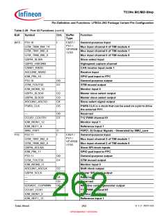
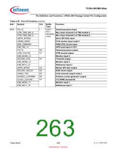
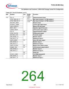
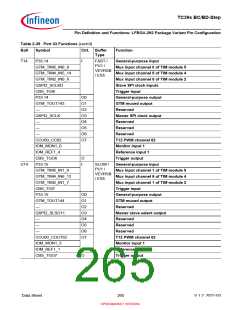
TC39x BC/BD-Step
Pin Definition and Functions: LFBGA-292 Package Variant Pin Configuration
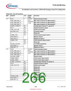
Table 2-39 Port 33 Functions (cont’d)
Ball
Symbol
Ctrl. Buffer
Type
Function
W15
P33.10
I
FAST /
PU1 /
VEVRSB
/ ES5
General-purpose input
GTM_TIM4_IN4_14
GTM_TIM1_IN0_9
GTM_TIM0_IN0_9
QSPI4_SLSIA
QSPI3_HSICINB
CAN01_RXDD
ASCLIN0_ARXD
IOM_PIN_10
Mux input channel 4 of TIM module 4
Mux input channel 0 of TIM module 1
Mux input channel 0 of TIM module 0
Slave select input
Highspeed capture channel
CAN receive input node 1
Receive input
GPIO pad input to FPC
P33.10
O0
O1
General-purpose output
GTM muxed output
GTM_TOUT32
IOM_MON0_10
QSPI1_SLSO6
QSPI4_SLSO0
ASCLIN1_ASLSO
PSI5S_CLK
Monitor input 0
O2
O3
O4
O5
Master slave select output
Master slave select output
Slave select signal output
PSI5S CLK is a clock that can be used on a pin to drive
the external PHY.
—
O6
O7
Reserved
CCU61_COUT61
IOM_MON1_12
IOM_REF1_9
SMU_FSP1
P33.11
T12 PWM channel 61
Monitor input 1
Reference input 1
O
I
FSP[1..0] Output Signals - Generated by SMU_core
General-purpose input
Mux input channel 2 of TIM module 1
Mux input channel 2 of TIM module 0
Slave SPI clock inputs
GPIO pad input to FPC
General-purpose output
GTM muxed output
Y15
FAST /
PU1 /
VEVRSB
/ ES5
GTM_TIM1_IN2_8
GTM_TIM0_IN2_8
QSPI4_SCLKA
IOM_PIN_11
P33.11
O0
O1
GTM_TOUT33
IOM_MON0_11
ASCLIN1_ASCLK
QSPI4_SCLK
—
Monitor input 0
O2
O3
O4
O5
O6
O7
Shift clock output
Master SPI clock output
Reserved
—
Reserved
EDSADC_CGPWMN
CCU61_CC61
IOM_MON1_9
IOM_REF1_12
Negative carrier generator output
T12 PWM channel 61
Monitor input 1
Reference input 1
Data Sheet
262
V 1.2, 2021-03
OPEN MARKET VERSION

 INFINEON [ Infineon ]