TC1767
Electrical Parameters
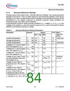
5.1.3
Absolute Maximum Ratings
Stresses above those listed under “Absolute Maximum Ratings” may cause permanent
damage to the device. This is a stress rating only and functional operation of the device
at these or any other conditions above those indicated in the operational sections of this
specification is not implied. Exposure to absolute maximum rating conditions for
extended periods may affect device reliability.
During absolute maximum rating overload conditions (VIN > related VDD or VIN < VSS) the
voltage on the related VDD pins with respect to ground (VSS) must not exceed the values
defined by the absolute maximum ratings.
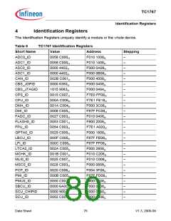
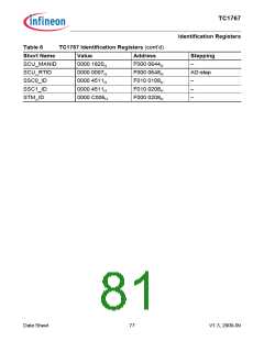
Table 8
Absolute Maximum Rating Parameters
Symbol Values
Min. Typ. Max.
Parameter
Unit Note /
Test Con
dition
Ambient temperature
Storage temperature
Junction temperature
TA
TST
TJ
SR -40
–
–
–
–
125
150
150
2.25
°C
°C
°C
V
Under bias
SR -65
SR -40
–
Under bias
–
Voltage at 1.5 V power supply VDD
pins with respect to VSS
–
1)
SR
Voltage at 3.3 V power supply VDDP SR –
pins with respect to VSS
–
–
3.75
5.5
V
V
V
–
–
2)
Voltage at 5 V power supply VDDM SR –
pins with respect to VSS
Voltage on any Class A input VIN
pin and dedicated input pins
with respect to VSS
SR -0.5 –
V
DDP + 0.5
Whatever
is lower
or max. 3.7
Voltage on any Class D
analog input pin with respect VAREFx
to VAGND
VAIN
-0.5 –
V
V
DDM + 0.5
DDM + 0.5
V
V
–
–
SR
Voltage on any Class D
VAINF
-0.5 –
analog input pin with respect VFAREF
to VSSAF, if the FADC is
SR
switched through to the pin.
1) Applicable for VDD, VDDOSC, VDDPLL, and VDDAF
.
2) Applicable for VDDP, VDDFL3, and VDDMF
.
Data Sheet
80
V1.3, 2009-09

 INFINEON [ Infineon ]