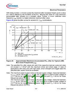
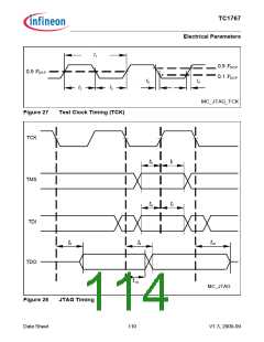
TC1767
Electrical Parameters
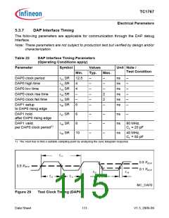
5.3.7
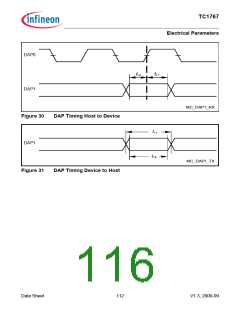
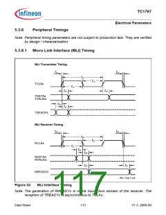
DAP Interface Timing
The following parameters are applicable for communication through the DAP debug
interface.
Note: These parameters are not subject to production test but verified by design and/or
characterization.
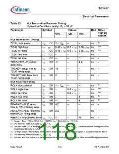
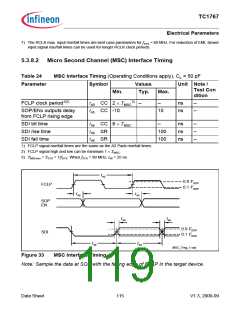
Table 22
DAP Interface Timing Parameters
(Operating Conditions apply)
Parameter
Symbol
Values
Unit Note /
Test Condition
Min.
Typ.
Max.
DAP0 clock period
DAP0 high time
t11 SR
t12 SR
t13 SR
t14 SR
t15 SR
t16 SR
12.5
–
–
–
–
–
–
–
–
–
2
2
–
ns
ns
ns
ns
ns
ns
–
4
4
–
–
6
–
–
–
–
–
DAP0 low time
DAP0 clock rise time
DAP0 clock fall time
DAP1 setup
to DAP0 rising edge
DAP1 hold
after DAP0 rising edge
t17 SR
t19 SR
t19 SR
6
–
–
–
–
–
–
ns
ns
ns
–
DAP1 valid
8
80 MHz,
CL = 20 pF
per DAP0 clock period1)
10
40 MHz,
CL = 50 pF
1) The Host has to find a suitable sampling point by analyzing the sync telegram response.
t11
0.9 VDDP
0.1 VDDP
0.5 VDDP
t15
t14
t12
t13
MC_DAP0
Figure 29
Test Clock Timing (DAP0)
Data Sheet
111
V1.3, 2009-09

 INFINEON [ Infineon ]