SAB 80C515/80C535
CPU
The SAB 80C515 is efficient both as a controller and as an arithmetic processor. It has
extensive facilities for binary and BCD arithmetic and excels in its bit-handling capabilities.
Efficient use of program memory results from an instruction set consisting of 44 % one-byte,
41 % two-byte, and 15 % three-byte instructions. With a 12 MHz crystal, 58 % of the
instructions execute in 1.0 µs.
Memory Organization
The SAB 80C515 manipulates operands in the four memory address spaces described below:
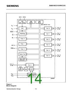
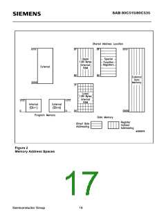
Figure 1 illustrates the memory address spaces of the SAB 80C515.
Program Memory
The SAB 80C515 has 8 Kbyte of on-chip ROM, while the SAB 80C535 has no internal ROM.
The program memory can be externally expanded up to 64 Kbytes. If the EA pin is held high,
the SAB 80C515 executes out of internal ROM unless the address exceeds 1FFF . Locations
H
2000 through 0FFFF are then fetched from the external program memory. If the EA pin is
H
H
held now, the SAB 80C515 fetches all instructions from the external program memory. Since
the SAB 80C535 has no internal ROM, pin EA must be tied low when using this component.
Data Memory
The data memory address space consists of an internal and an external memory space. The
internal data memory is divided into three physically separate and distinct blocks:
the lower 128 bytes of RAM, the upper 128 bytes of RAM, and the 128 byte special function
register (SRF) area. While the upper 128 bytes of data memory and the SFR area share the
same address locations, they are accessed through different addressing modes. The lower
128 bytes of data memory can be accessed through direct or register indirect addressing; the
upper 128 bytes of RAM can be accessed through register indirect addressing; the special
function registers are accessible through direct addressing.
Four 8-register banks, each bank consisting of eight 8-bit multi-purpose registers, occupy loca-
tions 0 through 1F in the lower RAM area. The next 16 bytes, locations 20 through 2F , con-
H
H
H
tain 128 directly addressable bit locations. The stack can be located anywhere in the internal
data memory address space, and the stack depth can be expanded up to 256 bytes.
The external data memory can be expanded up to 64 Kbytes and can be accessed by instruc-
tions that use a 16-bit or an 8-bit address.
Semiconductor Group
15

 INFINEON [ Infineon ]