CoolSET®-F3R
ICE3BR0665JF
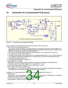
Schematic for recommended PCB layout
10
Schematic for recommended PCB layout
TR1
BR1
C12
R11
D21
Spark Gap 3
C11
bulk cap
FUSE1
X-CAP
C1
Vo
L
L1
D11
Spark Gap 1
C21
GND
Spark Gap 2
D11
Z11
Spark Gap 4
GND
N
IC11
R12
C3
C2
Y-CAP
C16
D13
R21
CS
DRAIN
VCC
R13
Y-CAP
C4
R14
F3
CoolSET
Y-CAP
BA
R23
R22
C23
GND
FB
NC
C22
C15
C13
C14
R24
*
IC12
IC21
R25
F3 CoolSET schematic for recommended PCB layout
Figure 72
Schematic for recommended PCB layout
General guideline for PCB layout design using F3/F3R CoolSET (refer to Figure 72):
1. “Star Ground “at bulk capacitor ground, C11:
“Star Ground “means all primary DC grounds should be connected to the ground of bulk capacitor C11
separately in one point. It can reduce the switching noise going into the sensitive pins of the CoolSET device
effectively. The primary DC grounds include the followings.
a. DC ground of the primary auxiliary winding in power transformer, TR1, and ground of C16 and Z11.
b. DC ground of the current sense resistor, R12
c. DC ground of the CoolSET device, GND pin of IC11; the signal grounds from C13, C14, C15 and collector of
IC12 should be connected to the GND pin of IC11 and then “star “connect to the bulk capacitor ground.
d. DC ground from bridge rectifier, BR1
e. DC ground from the bridging Y-capacitor, C4
2. High voltage traces clearance:
High voltage traces should keep enough spacing to the nearby traces. Otherwise, arcing would incur.
a. 400V traces (positive rail of bulk capacitor C11) to nearby trace: > 2.0mm
b. 600V traces (drain voltage of CoolSET IC11) to nearby trace: > 2.5mm
3. Filter capacitor close to the controller ground:
Filter capacitors, C13, C14 and C15 should be placed as close to the controller ground and the controller pin
as possible so as to reduce the switching noise coupled into the controller.
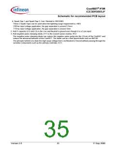
Guideline for PCB layout design when >3KV lightning surge test applied (refer to Figure 72):
1. Add spark gap
Spark gap is a pair of saw-tooth like copper plate facing each other which can discharge the accumulated
charge during surge test through the sharp point of the saw-tooth plate.
a. Spark Gap 3 and Spark Gap 4, input common mode choke, L1:
Gap separation is around 1.5mm (no safety concern)
Version 2.0
34
11 Sep 2008

 INFINEON [ Infineon ]