High Current PN Half Bridge
BTS 7960
Application
6
Application
6.1
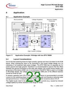
Application Example
Microcontroller
Voltage Regulator
Reverse Polarity
Protection
I/O
Reset
Vdd
WO
RO
Q
TLE
4278G
I
µC
VS
D
GND
SPD
Vss
I/O I/O I/O I/O
50P03L
BTS 7960B
BTS 7960B
VS
VS
INH
IN
INH
IN
M
OUT
GND
OUT
GND
IS
IS
SR
SR
High Current H-Bridge
Figure 11
6.2
Application Example: H-Bridge with two BTS 7960B
Layout Considerations
Due to the fast switching times for high currents, special care has to be taken to the PCB
layout. Stray inductances have to be minimized in the power bridge design as it is
necessary in all switched high power bridges. The BTS 7960 has no separate pin for
power ground and logic ground. Therefore it is recommended to assure that the offset
between the ground connection of the slew rate resistor, the current sense resistor and
ground pin of the device (GND / pin 1) is minimized. If the BTS 7960 is used in a H-bridge
or B6 bridge design, the voltage offset between the GND pins of the different devices
should be small as well.
A ceramic capacitor from VS to GND close to each device is recommended to provide
current for the switching phase via a low inductance path and therefore reducing noise
and ground bounce. A reasonable value for this capacitor would be about 470 nF.
The digital inputs need to be protected from excess currents (e.g. caused by induced
voltage spikes) by series resistors in the range of 10 kΩ.
Data Sheet
22
Rev. 1.1, 2004-12-07

 INFINEON [ Infineon ]