Data sheet BTS 6163 D
V
disconnect with energised inductive
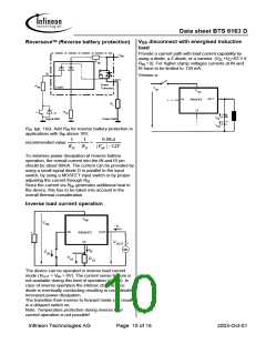
Reversave (Reverse battery protection)
bb
load
Provide a current path with load current capability by
using a diode, a Z-diode, or a varistor. (V +V <63 V if
V
-
bb
ZL
D
R
bb
R
=0). For higher clamp voltages currents at IN and
IN
IS have to be limited to 120 mA.
IN
Version a:
OUT
Power
Transistor
R
Logic
IN
V
bb
V
bb
OUT
IN
PROFET
R
L
IS
R
D
IS
V
V
Signal GND
Power GND
D
ZL
R
typ. 1kΩ. Add R for reverse battery protection in
applications with V above 16V;
bb
IS
IN
1
1
0.08A
|Vbb | −12V
recommended value:
+
=
RIN RIS
To minimise power dissipation at reverse battery
operation, the overall current into the IN and IS pin
should be about 80mA. The current can be provided by
using a small signal diode D in parallel to the input
switch, by using a MOSFET input switch or by proper
adjusting the current through R
IS.
Since the current via R generates additional heat in
bb
the device, this has to be taken into account in the
overall thermal consideration.
Inverse load current operation
V
bb
V
bb
- I
L
OUT
IN
+
-
PROFET
IS
V
+
-
OUT
I
IS
V
IN
V
R
IS
IS
The device can be operated in inverse load current
mode (VOUT > Vbb > 0V). The current sense feature is
not available during this kind of operation (IIS = 0). In
case of inverse operation the intrinsic drain source
diode is eventually conducting resulting in considerably
increased power dissipation.
The transition from inverse to forward mode can result
in a delayed switch on.
Note: Temperature protection during inverse load
current operation is not possible!
Infineon Technologies AG
Page 10 of 16
2003-Oct-01

 INFINEON [ Infineon ]