IDT70V5388/78
3.3V 64/32K x 18 Synchronous FourPort™ Static RAM
Industrial and Commercial Temperature Ranges
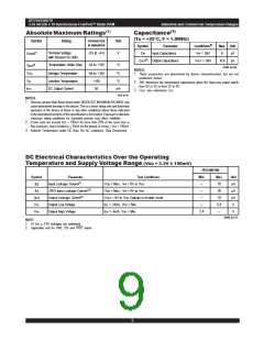
Capacitance(1)
AbsoluteMaximumRatings(1)
(TA = +25°C, F = 1.0MHZ)
Symbol
Rating
Commercial
& Industrial
Unit
V
Symbol
Parameter
Input Capacitance
Output Capacitance
Conditions(2)
IN = 3dV
OUT = 3dV
Max. Unit
(2 )
Terminal Voltage
with Respect to GND
-0.5 to +4.6
CIN
V
8
pF
pF
V
TERM
(3)
OUT
C
V
10.5
Temperature Under Bias
-55 to +125
oC
(3)
T
BIAS
STG
JN
OUT
5649 tbl 09
NOTES:
T
Storage Temperature
Junction Temperature
DC Output Current
-65 to +150
+150
oC
oC
1. These parameters are determined by device characterization, but are not
production tested.
2. 3dV references the interpolated capacitance when the input and output switch
from 0V to 3V or from 3V to 0V.
T
I
50
mA
3. COUT also references CI/O.
5623 tbl 06
NOTES:
1. Stresses greater than those listed under ABSOLUTE MAXIMUM RATINGS may
cause permanent damage to the device. This is a stress rating only and functional
operation of the device at these or any other conditions above those indicated
in the operational sections of this specification is not implied. Exposure to absolute
maximum rating conditions for extended periods may affect reliability.
2. VTERM must not exceed VDD + 150mV for more than 25% of the cycle time or
4ns maximum, and is limited to < 20mA for the period of VTERM > VDD + 150mV.
3. Ambient Temperature under DC Bias. No AC conditions. Chip Deselected.
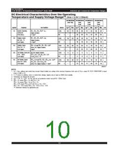
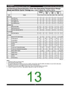
DC Electrical Characteristics Over the Operating
Temperature and Supply Voltage Range (VDD = 3.3V ± 150mV)
70V5388/78S
Symbol
Parameter
Input Leakage Current(1)
JTAG Input Leakage Current(1,2)
Output Leakage Current(1)
Output Low Voltage
Test Conditions
DD = Max., VIN = 0V to VDD
Min.
Max.
10
Unit
µA
µA
µA
V
___
___
___
___
|ILI
|ILI
|ILO
|
V
V
V
|
DD = Max., VIN = 0V to VDD
30
|
OUT = 0V to VDD, Outputs in tri-state mode
10
V
OL
OH
I
OL = +4mA, VDD = Min.
0.4
___
V
Output High Voltage
I
OH = -4mA, VDD = Min.
2.4
V
5649 tbl 10
NOTE:
1. At VDD < 2.0V leakages are undefined.
2. Applicable only for TMS, TDI and TRST inputs.
9
6.42

 IDT [ INTEGRATED DEVICE TECHNOLOGY ]