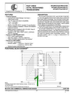
IDT29FCT52AT/BT/CT/DT, IDT29FCT/2052AT/BT/CT, IDT29FCT53AT/BT/CT
FAST CMOS OCTAL REGISTERED TRANSCEIVERS
MILITARY AND COMMERCIAL TEMPERATURE RANGES
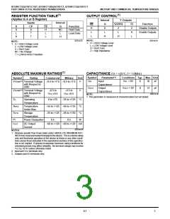
REGISTER FUNCTION TABLE(1)
(Applies to A or B Register)
OUTPUT CONTROL(1)
Internal
Y-Outputs
Inputs
Internal
Q
X
L
52/2052
53
Z
Function
OE
H
D
X
L
CP
X
Q
NC
L
Function
Hold Data
Load Data
CE
H
Z
L
Disable Outputs
Enable Outputs
L
H
L
↑
L
L
H
H
H
↑
L
H
NOTE:
2629 tbl 03
2629 tbl 02
NOTE:
1. H = HIGH Voltage Level
L = LOW Voltage Level
X = Don’t Care
1. H = HIGH Voltage Level
L = LOW Voltage Level
X = Don’t Care
Z = High Impedance
NC = No Change
↑ = LOW-to-HIGH Transition
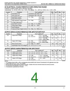
ABSOLUTE MAXIMUM RATINGS(1)
CAPACITANCE (TA = +25°C, f = 1.0MHz)
Symbol
Parameter(1)
Conditions Typ. Max. Unit
Symbol
Rating
Commercial
Military
Unit
(2)
CIN
Input
Capacitance
Output
VIN = 0V
6
8
10
pF
VTERM
Terminal Voltage
with Respect to
GND
–0.5 to +7.0 –0.5 to +7.0
V
COUT
VOUT = 0V
12
pF
(3)
VTERM
Terminal Voltage
with Respect to
GND
–0.5 to
–0.5 to
V
Capacitance
VCC +0.5
VCC +0.5
2640 lnk 05
NOTE:
1. This parameter is measured at characterization but not tested.
TA
Operating
0 to +70
–55 to +125 °C
Temperature
Temperature
Under Bias
Storage
TBIAS
TSTG
–55 to +125 –65 to +135 °C
–55 to +125 –65 to +150 °C
Temperature
Power Dissipation
PT
0.5
0.5
W
IOUT
DC Output
Current
–60 to +120 –60 to +120 mA
2529 lnk 04
NOTES:
1. Stresses greater than those listed under ABSOLUTE MAXIMUM RAT-
INGS may cause permanent damage to the device. This is a stress rating
only and functional operation of the device at these or any other condi-
tions above those indicated in the operational sections of this specifica-
tion is not implied. Exposure to absolute maximum rating conditions for
extended periods may affect reliability. No terminal voltage may exceed
VCC by +0.5V unless otherwise noted.
2. Input and VCC terminals only.
3. Outputs and I/O terminals only.
6.1
3

 IDT [ INTEGRATED DEVICE TECHNOLOGY ]