®
IS42S81600A, IS42S16800A, IS42S32400A
IS42LS81600A, IS42LS16800A, IS42LS32400A
ISSI
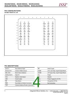
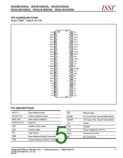
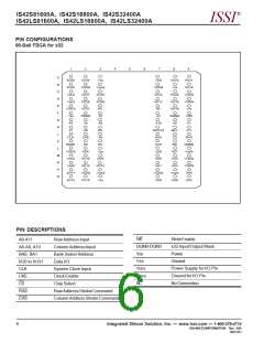
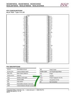
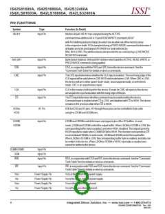
PIN FUNCTIONS
Symbol
Type
Function (In Detail)
A0-A11
Input Pin
AddressInputs:A0-A11aresampledduringtheACTIVE
command(row-addressA0-A11)andREAD/WRITEcommand(A0-A7
with A10 defining auto precharge) to select one location out of the memory array
intherespectivebank.A10issampledduringaPRECHARGEcommandtodetermineif
all banks are to be precharged (A10 HIGH) or bank selected by
BA0, BA1 (LOW). The address inputs also provide the op-code during a LOAD MODE
REGISTERcommand.
BA0, BA1
CAS
Input Pin
Input Pin
Input Pin
BankSelectAddress:BA0andBA1defineswhichbanktheACTIVE, READ, WRITEor
PRECHARGEcommandisbeingapplied.
CAS, inconjunctionwiththeRASand WE, formsthedevicecommand. Seethe
"CommandTruthTable"fordetailsondevicecommands.
CKE
TheCKEinputdetermineswhethertheCLKinputisenabled. Thenextrisingedgeofthe
CLKsignalwillbevalidwhenisCKEHIGHandinvalidwhenLOW. WhenCKEisLOW,
the device will be in either power-down mode, clock suspend mode, or self refresh
mode. CKE is an asynchronous input.
CLK
Input Pin
Input Pin
CLK is the master clock input for this device. Except for CKE, all inputs to this device
areacquiredinsynchronizationwiththerisingedgeofthispin.
CS
TheCSinputdetermineswhethercommandinputisenabledwithinthedevice.
Command input is enabled whenCSisLOW, anddisabledwithCSisHIGH. Thedevice
remains in the previous state when CS is HIGH.
I/O0 to
I/O32
I/O Pin
I/O0 to I/O32 are I/O pins. I/O through these pins can be controlled in byte units
using the LDQM and UDQM pins.
LDQM,
UDQM
Input Pin
LDQM and UDQM control the lower and upper bytes of the I/O buffers. In read
mode, LDQM and UDQM control the output buffer. When LDQM or UDQM is LOW, the
correspondingbufferbyteisenabled, andwhenHIGH, disabled. Theoutputsgotothe
HIGH impedance state when LDQM/UDQM is HIGH. This function corresponds to OE
inconventionalDRAMs. Inwritemode, LDQMandUDQMcontroltheinputbuffer.
When LDQM or UDQM is LOW, the corresponding buffer byte is enabled, and data can
be written to the device. When LDQM or UDQM is HIGH, input data is masked and
cannot be written to the device.
DQM0-DQM3
DQM
Input Pin
Input Pin
Input Pin
RAS
RAS,inconjunctionwithCASandWE,formsthedevicecommand.Seethe"Command
TruthTable"itemfordetailsondevicecommands.
WE
Input Pin
WE,inconjunctionwithRASandCAS,formsthedevicecommand.Seethe"Command
TruthTable"itemfordetailsondevicecommands.
VDDQ
VDD
Power Supply Pin
Power Supply Pin
Power Supply Pin
Power Supply Pin
VDDQ istheoutputbufferpowersupply.
VDD isthedeviceinternalpowersupply.
VSSQ istheoutputbufferground.
VSSQ
VSS
VSS isthedeviceinternalground.
8
Integrated Silicon Solution, Inc. — www.issi.com — 1-800-379-4774
ADVANCEDINFORMATION Rev. 00A
06/01/02

 ICSI [ INTEGRATED CIRCUIT SOLUTION INC ]