ICS91309
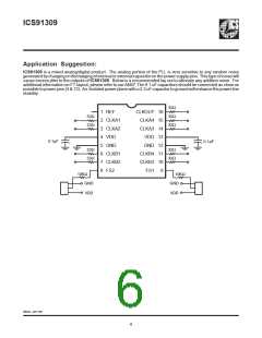
Application Suggestion:
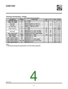
ICS91309 is a mixed analog/digital product. The analog portion of the PLL is very sensitive to any random noise
generated by charging or discharging of internal or external capacitor on the power supply pins. This type of noise will
cause excess jitter to the outputs of ICS91309. Below is a recommended lay out to alleviate any addition noise. For
additional information on FT.layout, please refer to our AN07.The 0.1 uF capacitors should be connected as close as
possible to power pins (4 & 13). An Isolated power plane with a 2.2 uF capacitor to ground will enhance the power line
stability.
33Ω
1 REF
CLKOUT 16
CLKA4 15
CLKA3 14
VDD 13
33Ω
33Ω
33Ω
33Ω
2 CLKA1
3 CLKA2
4 VDD
0.1µF
0.1µF
5 GND
GND 12
33Ω
33Ω
33Ω
33Ω
6 CLKB1
7 CLKB2
8 FS2
CLKB4 11
CLKB3 10
FS1
9
10KΩ
10KΩ
GND
VDD
GND
VDD
0093G—02/11/04
6

 ICSI [ INTEGRATED CIRCUIT SOLUTION INC ]