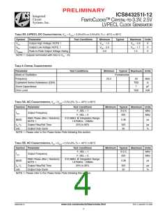
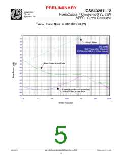
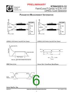
PRELIMINARY
ICS843251I-12
Integrated
Circuit
Systems, Inc.
FEMTOCLOCKS™ CRYSTAL-TO-3.3V, 2.5V
LVPECL CLOCK GENERATOR
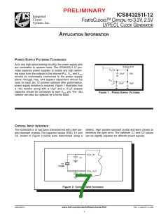
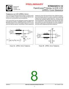
TERMINATION FOR 3.3V LVPECL OUTPUT
The clock layout topology shown below is a typical termi-
nation for LVPECL outputs. The two different layouts men-
tioned are recommended only as guidelines.
designed to drive 50Ω transmission lines. Matched imped-
ance techniques should be used to maximize operating
frequency and minimize signal distortion. Figures 3A and
3B show two different layouts which are recommended
only as guidelines. Other suitable clock layouts may exist
and it would be recommended that the board designers
simulate to guarantee compatibility across all printed cir-
cuit and clock component process variations.
FOUT and nFOUT are low impedance follower outputs that
generate ECL/LVPECL compatible outputs. Therefore, ter-
minating resistors (DC current path to ground) or current
sources must be used for functionality. These outputs are
3.3V
Zo = 50Ω
125Ω
125Ω
FOUT
FIN
Zo = 50Ω
Zo = 50Ω
Zo = 50Ω
FOUT
FIN
50Ω
50Ω
VCC - 2V
1
RTT =
Zo
RTT
((VOH + VOL) / (VCC – 2)) – 2
84Ω
84Ω
FIGURE 3A. LVPECL OUTPUT TERMINATION
FIGURE 3B. LVPECL OUTPUT TERMINATION
843251BGI-12
www.icst.com/products/hiperclocks.html
REV.A JANUARY 10, 2006
8

 ICSI [ INTEGRATED CIRCUIT SOLUTION INC ]