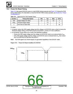
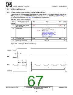
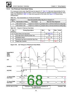
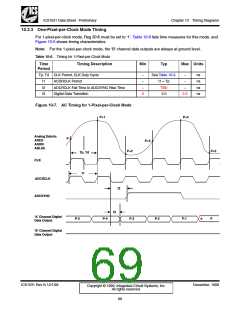
ICS1531 Data Sheet - Preliminary
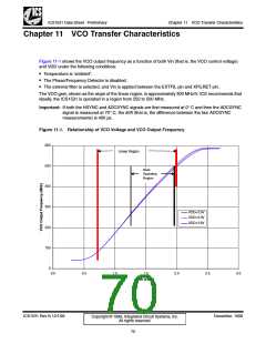
Chapter 11 VCO Transfer Characteristics
Chapter 11 VCO Transfer Characteristics
Figure 11-1 shows the VCO output frequency as a function of both Vin (that is, the VCO control voltage)
and VDD under the following conditions:
• Temperature is ‘ambient’.
• The Phase/Frequency Detector is disabled.
• The external filter is selected, and Vin is applied between the EXTFIL pin and XFILRET pin.
The VCO gain, shown as the slope of the linear region, is approximately 300 MHz/V. ICS recommends that
ideally, the ICS1531 is operated in a region from 250 to 500 MHz.
Important: If both the HSYNC and ADCSYNC signals are first measured at 0° C and then the ADCSYNC
signal is measured at 70° C, the drift (that is, the difference between the two ADCSYNC
measurements) is 400 ps.
Figure 11-1. Relationship of VCO Voltage and VCO Output Frequency
600
Linear Region
500
Ideal
Operating
Region
400
300
VDD=3.0V
VDD=3.3V
VDD=3.6V
200
100
0
0.0
0.5
1.0
1.5
2.0
2.5
3.0
Vin (Volts)
ICS1531 Rev N 12/1/99
December, 1999
Copyright © 1999, Integrated Circuit Systems, Inc.
All rights reserved.
70

 ICSI [ INTEGRATED CIRCUIT SOLUTION INC ]