ICS1531 Data Sheet - Preliminary
Chapter 10 Timing Diagrams
10.3 AC Timing Diagrams
10.3.1 Phase-Locked-Loop Timing for Digital Setup and Hold
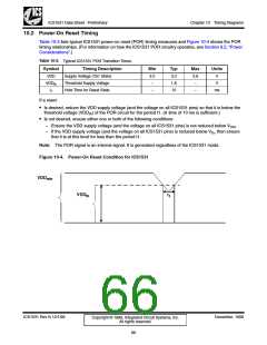
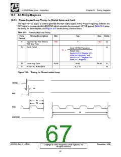
The input HSYNC signal is used to generate the REF output signal. In the Phase/Frequency Detector, the
REF signal is compared with ADCSYNC (which provides the recovered HSYNC signal). Table 10-3 gives
the timing for these signals, and Figure 10-5 shows timing characteristics.
Table 10-3. Phase-Locked-Loop Timing
Time
Timing Description
Min
Typ
Max Units
Period
t1
Input HSYNC Rise Time to
REF Rise Time
TBD
7
TBD
ns
ns
Tp
Clock Period
Input HSYNC Frequency
Tp
=
Result from:
Section 6.5.3, “Register 02h:
Fdbk Div 0 Register” and
Section 6.5.4, “Register 03h:
Fdbk Div 1 Register”
Td
t2
Clock Duty Cycle
45-55
50-50
55-45
%
ADCSYNC Active Time
4 × Tp
ns
Figure 10-5. Timing for Phase-Locked Loop
HSYNC
REF
t1
Tp
Td
CLK
t2
ADCSYNC
ICS1531 Rev N 12/1/99
December, 1999
Copyright © 1999, Integrated Circuit Systems, Inc.
All rights reserved.
67

 ICSI [ INTEGRATED CIRCUIT SOLUTION INC ]