ICS1531 Data Sheet - Preliminary
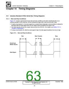
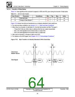
Chapter 10 Timing Diagrams
10.2 Power-On Reset Timing
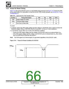
Table 10-2 lists typical ICS1531 power-on reset (POR) timing measures and Figure 10-4 shows the POR
timing relationships. (For information on how the ICS1531 POR circuitry operates, see Section 8.2, “Power
Considerations”.)
Table 10-2. Typical ICS1531 POR Transition Times
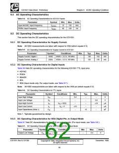
Symbol
VDD
Timing Description
Supply Voltage (‘On’ State)
Min
3.0
–
Typ
3.3
1.8
10
Max
3.6
–
Units
V
VDDth
t1
Threshold Supply Voltage
Hold Time for Reset State
V
–
–
ms
If a reset:
• Is desired, reduce the VDD supply voltage (and the voltage on all ICS1531 pins) so that it is below the
threshold voltage (VDDth) of the POR circuit for the period t1. (A time of 10 ms is sufficient.)
• Is not desired, ensure either one or both of the following conditions:
– Ensure the VDD supply voltage (and the voltage on all ICS1531 pins) is not reduced below Vmin
.
– If the VDD supply voltage (and the voltage on all ICS1531 pins) is reduced below Vth, then ensure
that it is at this level for less than the period t1.
Note: The POR signal is an internal signal. It is generated regardless of the ICS1531 mode.
Figure 10-4. Power-On Reset Condition for ICS1531
VDDmin
VDDth
t1
ICS1531 Rev N 12/1/99
December, 1999
Copyright © 1999, Integrated Circuit Systems, Inc.
All rights reserved.
66

 ICSI [ INTEGRATED CIRCUIT SOLUTION INC ]