ICS1531 Data Sheet - Preliminary
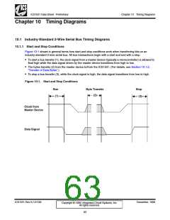
Chapter 10 Timing Diagrams
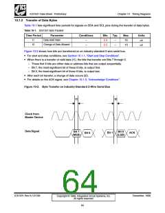
10.1.2 Transfer of Data Bytes
Table 10-1 lists significant time periods for signals on SDA and SCL pins during the transfer of data bytes.
Table 10-1. ICS1531 Byte Transfer
Time Period
Parameter
Data Held Valid
Change of Data Allowed
Conditions
Min.
2.5
Typ.
Max.
10
Units
µs
t1
t2
–
–
–
–
2.5
10
µs
Figure 10-2 shows how bits are transferred on an industry-standard 2-wire serial bus.
• For start and stop conditions, see Section 10.1.1, “Start and Stop Conditions”.
• When there is a transfer of valid data (t1), the bits that transfer are Bits 7 through 0.
– These first 8 bits are either data or address bits that are output sequentially.
– Bit 7, the most-significant bit of these 8 bits, is output first.
– Bit 0, the least-significant bit of these 8 bits, is output last.
• After each bit transfer, a change of data occurs (t2).
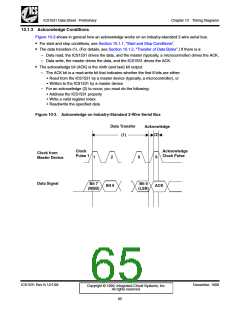
• For details on the ACK signal, see Chapter 10.1.3, “Acknowledge Conditions”.
Figure 10-2. Byte Transfer on Industry-Standard 2-Wire Serial Bus
t1
t2
Clock from
Master Device
Data Signal
Bit 7
(MSB)
Bit 0
(LSB)
ACK
Bit 1
Bit 6
ICS1531 Rev N 12/1/99
December, 1999
Copyright © 1999, Integrated Circuit Systems, Inc.
All rights reserved.
64

 ICSI [ INTEGRATED CIRCUIT SOLUTION INC ]