iC-HC
ULTRA FAST DUAL HV-KOMPARATOR
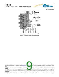
Rev A1, Page 3/10
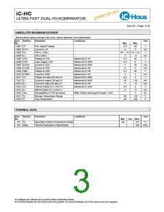
ABSOLUTE MAXIMUM RATINGS
Beyond these values damage may occur; device operation is not guaranteed.
Item Symbol
No.
Parameter
Conditions
Unit
Min.
-0.5
-5
Max.
G001 VP
G002 I(VP)
G003 V()
G004 I()
Pos. Supply Voltage
Current in VP
46
5
V
mA
V
V(IPx), V(INx)
VN − 0.5 VP + 0.5
I(IPx), I(INx)
-2
-0.5
-0.5
-5
+2
46
6
mA
V
G005 VDD
G006 VDD
G007 I(VDD)
G008 I(VDD)
G009 GND
G010 I(GND)
G011 V()
G012 I()
Voltage at VDD
referenced to VN
referenced to GND
referenced to GND
referenced to VN
referenced to VN
referenced to VN
referenced to GND
referenced to GND
referenced to VN
referenced to GND
Logic Supply VDD
V
Current in VDD
20
5
mA
mA
V
Current in VDD
-5
Voltage at GND
-0.5
-5
46
5
Current in GND
mA
V
Voltage at output O0 and O1
Current in output O0 and O1
Current in iutput O0 and O1
V(NFAST,NEN,T0,T1,P0,P1)
I(NFAST,NEN,T0,T1,P0,P1)
Susceptibility to ESD at all pins
Storage Temperature Range
Chip Temperature
-0.5
-20
-5
6
+20
+5
6
mA
mA
V
G013 I()
G014 V()
G015 I()
-0.5
-5
+5
3
mA
kV
°C
°C
G016 Vd()
G017 Ts
HBM, 100 pF discharged through 1.5 kΩ
-40
-40
150
150
G018 Tj
THERMAL DATA
Item Symbol
No.
Parameter
Conditions
Unit
Min. Typ. Max.
T01 Ta
Operating Ambient Temperature Range
Thermal Resistance Chip/Ambient
-40
125
140
°C
T02 Rthja
K/W
All voltages are referenced to ground unless otherwise stated.
All currents flowing into the device pins are positive; all currents flowing out of the device pins are negative.

 ICHAUS [ IC-HAUS GMBH ]