Si4430/31/32-B1
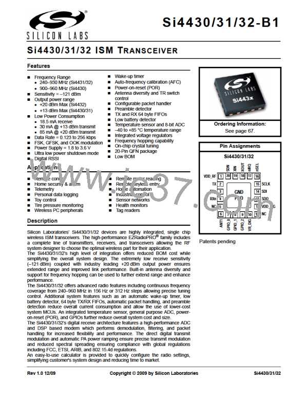
13. Pin Descriptions: Si4430/31/32
20 19 18 17
VDD_RF
TX
1
16
2
15 SCLK
14 SDI
13 SDO
12 VDD_DIG
11 NC
RXp
RXn
NC
3
4
5
GND
PAD
6
7
8
9
10
Pin
Pin Name
I/O
Description
1
VDD_RF
VDD +1.8 to +3.6 V supply voltage input to all analog +1.7 V regulators. The recommended VDD supply voltage
is +3.3 V.
2
TX
O
Transmit output pin. The PA output is an open-drain connection so the L-C match must supply VDD
(+3.3 VDC nominal) to this pin.
3
4
5
6
7
8
9
RXp
RXn
I
Differential RF input pins of the LNA. See application schematic for example matching network.
I
NC
—
O
No Connect. Not connected internally to any circuitry.
ANT1
GPIO_0
GPIO_1
GPIO_2
Extra antenna or TR switch control to be used if more GPIO are required. See register description of 08h.
I/O
I/O
I/O
General Purpose Digital I/O that may be configured through the registers to perform various functions
including: Microcontroller Clock Output, FIFO status, POR, Wake-Up timer, Low Battery Detect, TRSW,
AntDiversity control, etc. See the SPI GPIO Configuration Registers, Address 0Bh, 0Ch, and 0Dh for
more information.
10
11
VR_DIG
NC
O
Regulated Output Voltage of the Digital 1.7 V Regulator. A 1 µF decoupling capacitor is required.
—
Internally this pin is tied to the paddle of the package. This pin should be left unconnected or connected to
GND only.
12
VDD_DIG
VDD +1.8 to +3.6 V supply voltage input to the Digital +1.7 V Regulator. The recommended VDD supply voltage
is +3.3 V.
13
14
SDO
SDI
O
I
0–VDD V digital output that provides a serial readback function of the internal control registers.
Serial Data input. 0–VDD V digital input. This pin provides the serial data stream for the 4-line serial data
bus.
15
16
17
SCLK
nSEL
nIRQ
I
I
Serial Clock input. 0–VDD V digital input. This pin provides the serial data clock function for the 4-line
serial data bus. Data is clocked into the Si4430/31/32 on positive edge transitions.
Serial Interface Select input. 0– VDD V digital input. This pin provides the Select/Enable function for the 4-
line serial data bus. The signal is also used to signify burst read/write mode.
O
General Microcontroller Interrupt Status output. When the Si4430/31/32 exhibits anyone of the Interrupt
Events the nIRQ pin will be set low=0. Please see the Control Logic registers section for more information
on the Interrupt Events. The Microcontroller can then determine the state of the interrupt by reading a cor-
responding SPI Interrupt Status Registers, Address 03h and 04h. No external resistor pull-up is required,
but it may be desirable if multiple interrupt lines are connected.
18
XOUT
O
Crystal Oscillator Output. Connect to an external 30 MHz crystal or to an external source. If using an
external source with no crystal then dc coupling with a nominal 0.8 VDC level is recommended with a
minimum amplitude of 700 mVpp.
19
20
XIN
SDN
I
I
Crystal Oscillator Input. Connect to an external 30 MHz crystal or leave floating when driving with an
external source on XOUT..
Shutdown input pin. 0–VDD V digital input. SDN should be = 0 in all modes except Shutdown mode. When
SDN =1 the chip will be completely shutdown and the contents of the registers will be lost.
PKG
PADDLE_GND
GND The exposed metal paddle on the bottom of the Si4430/31/32 supplies the RF and circuit ground(s) for the
entire chip. It is very important that a good solder connection is made between this exposed metal paddle
and the ground plane of the PCB underlying the Si4430/31/32.
66
Rev 1.0

 IBM [ IBM ]