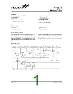
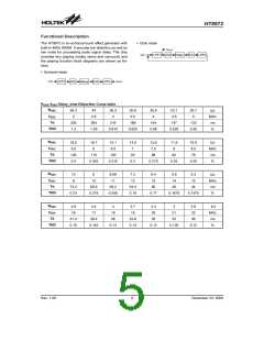
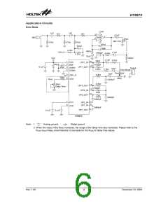
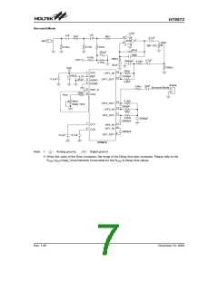
HT8972
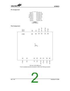
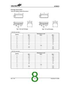
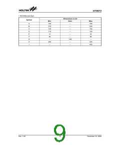
Pad Coordinates
Unit: mm
Pad No.
X
Y
Pad No.
X
Y
1
2
3
4
5
6
7
8
861.250
-891.900
-892.700
-892.700
-892.700
-892.700
-892.700
-892.700
9
1027.425
907.375
715.175
467.375
275.175
60.790
-883.875
-865.105
-564.105
-44.775
147.425
395.225
587.425
835.225
-892.700
10
11
12
13
14
15
16
890.431
890.429
890.431
890.429
879.700
868.440
861.250
-203.150
-783.875
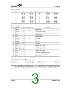
Pad Description
Pad No. Pad Name
I/O Internal Connection
Description
1
2
DGND
I
O
I
Digital ground
¾
¾
¾
¾
¾
¾
¾
¾
¾
¾
¾
¾
¾
¾
¾
¾
OSC_O
VCO
System oscillator output
3
System oscillator input, system frequency adjustable pin
Current control 1
4
CC1
¾
¾
O
I
5
CC0
Current control 0
6
OP1_OUT
OP1_IN
OP2_IN
OP2_OUT
LPF2_IN
LPF2_OUT
LPF1_OUT
LPF1_IN
VCC
OP1 output
7
OP1 input
8
I
OP2 input
9
O
I
OP2 output
10
11
12
13
14
15
16
Low pass filter 2 input
Low pass filter 2 output
Low pass filter 1 output
Low pass filter 1 input
Analog and positive power supply
Analog reference voltage
Analog ground
O
O
I
I
REF
I
AGND
I
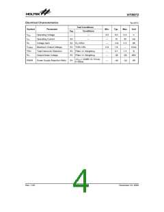
Absolute Maximum Ratings
Supply Voltage...........................VSS-0.3V to VSS+6.0V
Input Voltage..............................VSS-0.3V to VDD+0.3V
Storage Temperature............................-50°C to 125°C
Operating Temperature .............................-20°C to 70°
Note: These are stress ratings only. Stresses exceeding the range specified under ²Absolute Maximum Ratings² may
cause substantial damage to the device. Functional operation of this device at other conditions beyond those listed
in the specification is not implied and prolonged exposure to extreme conditions may affect device reliability.
Rev. 1.00
3
December 23, 2008

 HOLTEK [ HOLTEK SEMICONDUCTOR INC ]