HT75XX-2
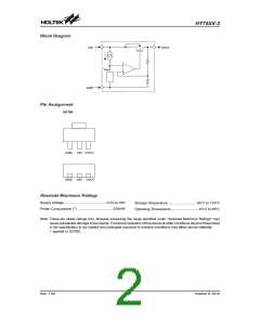
Pin Descriptions
Pin No.
Pin Name
GND
Pin Description
1
2
3
Ground pin
Input pin
VIN
VOUT
Output pin
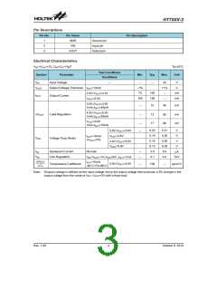
Electrical Characteristics
VIN =VOUT+2V, CIN=CO=10mF
Ta=25°C
Test Conditions
Symbol
Parameter
Input Voltage
Output Voltage Tolerance IOUT=10mA
3.0V£VOUT£4.4V
OUT=5.0V
Min.
Typ.
Max.
Unit
Conditions
VIN
24
+1%
¾
V
V
¾
¾
-1%
70
¾
VOUT
100
150
mA
mA
IOUT
Output Current
100
V
¾
3.0V£VOUT£3.6V
1mA£IOUT£50mA
10
13
17
45
65
80
mV
mV
mV
¾
¾
¾
4.0V£VOUT£5.0V
1mA£IOUT£50mA
DVOUT
Load Regulation
VOUT=5.0V
1mA£IOUT£70mA
0.23
0.19
0.16
0.12
2.5
0.41
0.35
0.30
0.25
5.0
V
V
3.0V£VOUT<3.6V
OUT=3.6V
¾
V
IOUT=10mA,
VDIF
Voltage Drop (Note)
DVOUT=2%
V
4.0V£VOUT<5.0V
OUT=5.0V
V
V
ISS
Quiescent Current
Line Regulation
No load
¾
¾
mA
%/V
VIN
0.1
0.2
VIN=VOUT+1V£VIN£24V, IOUT=1mA
OUT=10mA
-40°C<Ta<85°C
D
V
O
U
T
I
3.0V£VOUT£5.0V
Temperature Coefficient
100
¾
¾
ppm/°C
D
T
a
Note: Dropout voltage is defined as the input voltage minus the output voltage that produces a 2% change in the
output voltage from the value at VIN = VOUT+2V with a fixed load.
Rev. 1.00
3
October 6, 2010

 HOLTEK [ HOLTEK SEMICONDUCTOR INC ]