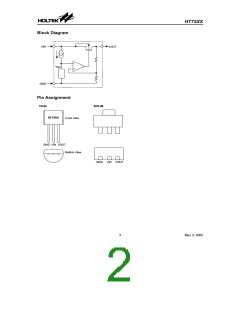
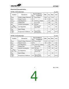
HT75XX
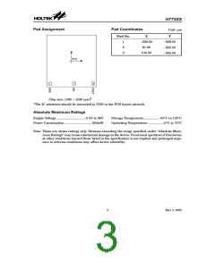
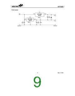
Pad Assignment
Pad Coordinates
Unit: mm
Pad No.
X
Y
1
2
3
-506.50
61.00
-589.50
-582.50
-585.50
510.50
(
0
,
0
)
2
3
1
Chip size: 1390 ´ 1530 (mm)2
*The IC substrate should be connected to VDD in the PCB layout artwork.
Absolute Maximum Ratings
Supply Voltage...............................-0.3V to 26V
Storage Temperature.................-50°C to 125°C
Operating Temperature ..................0°C to 70°C
Power Consumption.............................. 250mW
Note: These are stress ratings only. Stresses exceeding the range specified under ²Absolute Maxi-
mum Ratings² may cause substantial damage to the device. Functional operation of this device
at other conditions beyond those listed in the specification is not implied and prolonged expo-
sure to extreme conditions may affect device reliability.
3
May 2, 2000

 HOLTEK [ HOLTEK SEMICONDUCTOR INC ]