HT75XX-1
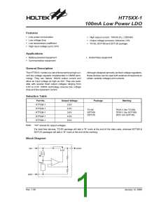
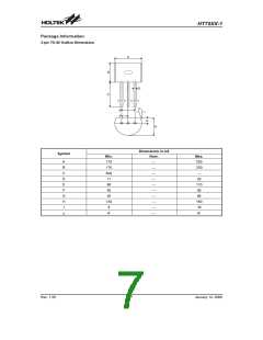
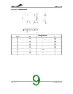
Pin Assignment
T
O
-
9
2
S
O
T
-
8
9
S
O
T
-
2
5
N
C
N
C
F
r
o
n
t
V
i
e
w
7
5
X
X
-
1
7
5
X
X
-
1
T
o
p
V
i
e
w
5
X
X
1
G
N
D
V
I
N
V
O
U
T
G
N
D
V
I
N
V
O
U
T
G
N
D
V
I
N
V
O
U
T
B
o
t
t
o
m
V
i
e
w
G
N
D
V
I
N
V
O
U
T
G
N
D
V
I
N
V
O
U
T
Absolute Maximum Ratings
Supply Voltage ..........................................-0.3V to 26V
Power Consumption (*1) .................................. 250mW
Power Consumption (*2) .................................. 150mW
Storage Temperature............................-50°C to 125°C
Operating Temperature...........................-40°C to 85°C
Note: These are stress ratings only. Stresses exceeding the range specified under ²Absolute Maximum Ratings² may
cause substantial damage to the device. Functional operation of this device at other conditions beyond those
listed in the specification is not implied and prolonged exposure to extreme conditions may affect device reliabil-
ity.
*1: applied to SOT89 and TO-92
*2: applied to SOT-25
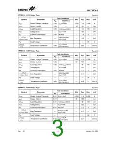
Electrical Characteristics
HT7530-1, +3.0V Output Type
Ta=25°C
Test Conditions
Conditions
Symbol
VOUT
Parameter
Min.
Typ.
Max.
Unit
VIN
5V
5V
5V
¾
Output Voltage Tolerance
Output Current
IOUT=10mA
2.91
60
3.0
100
60
3.09
¾
V
IOUT
mA
mV
mV
mA
¾
Load Regulation
150
¾
DVOUT
VDIF
ISS
1mA£IOUT£50mA
IOUT=1mA
Voltage Drop
100
2.5
¾
¾
Current Consumption
5V
No load
5
D
V
O U T
4V£VIN£24V
Line Regulation
0.2
¾
%/V
V
¾
¾
¾
¾
¾
¾
24
¾
I
OUT=1mA
D
I
N
´
O
U
T
VIN
Input Voltage
¾
D
V
O U T
IOUT=10mA
Temperature Coefficient
5V
±0.45
mV/°C
0°C<Ta<70°C
D
T
a
Rev. 1.50
2
January 12, 2006

 HOLTEK [ HOLTEK SEMICONDUCTOR INC ]